HMP8156 データシートの表示(PDF) - Intersil
部品番号
コンポーネント説明
メーカー
HMP8156 Datasheet PDF : 33 Pages
| |||
HMP8156
Video Timing Control
The pixel and overlay data must be presented to the
HMP8156 at 50 or 59.94 fields per second (interlaced). The
video timing is controlled by the BLANK, HSYNC, VSYNC,
FIELD, and CLK2 pins.
HSYNC
VSYNC
HSYNC, VSYNC, and FIELD Timing
The leading edge of HSYNC indicates the beginning of a
horizontal sync interval. If HSYNC is an output, it is asserted
for about 4.7 µs. If HSYNC is an input, it must be active for at
least two CLK2 periods. The width of the horizontal compos-
ite sync tip is determined from the video standard and does
not depend on the width of HSYNC.
The leading edge of VSYNC indicates the beginning of a
vertical sync interval. If VSYNC is an output, it is asserted for
3 scan lines in (M, NSM) NTSC and (M, N) PAL modes or
2.5 scan lines in (B, D, G, H, I, CN) PAL modes. If VSYNC is
an input, it must be asserted for at least two CLK2 periods.
When HSYNC and VSYNC are configured as outputs, their
leading edges will occur simultaneously at the start of an odd
field. At the start of an even field, the leading edge of
VSYNC occurs in the middle of the line.
When HSYNC and VSYNC are configured as inputs, if the
leading edge of HSYNC occurs within ±127 CLK2 cycles of
the leading edge of VSYNC, the encoder assumes it is at the
start of an odd field. Otherwise, it assumes it is processing
an even field.
The FIELD signal is always an output and changes state
near each leading edge of VSYNC. The delay between the
syncs and FIELD depends on the encoder’s operating mode
as summarized in Table 6. In modes in which the encoder
uses CLK to gate its inputs and outputs, the FIELD signal
may be delayed 0-12 additional CLK2 periods.
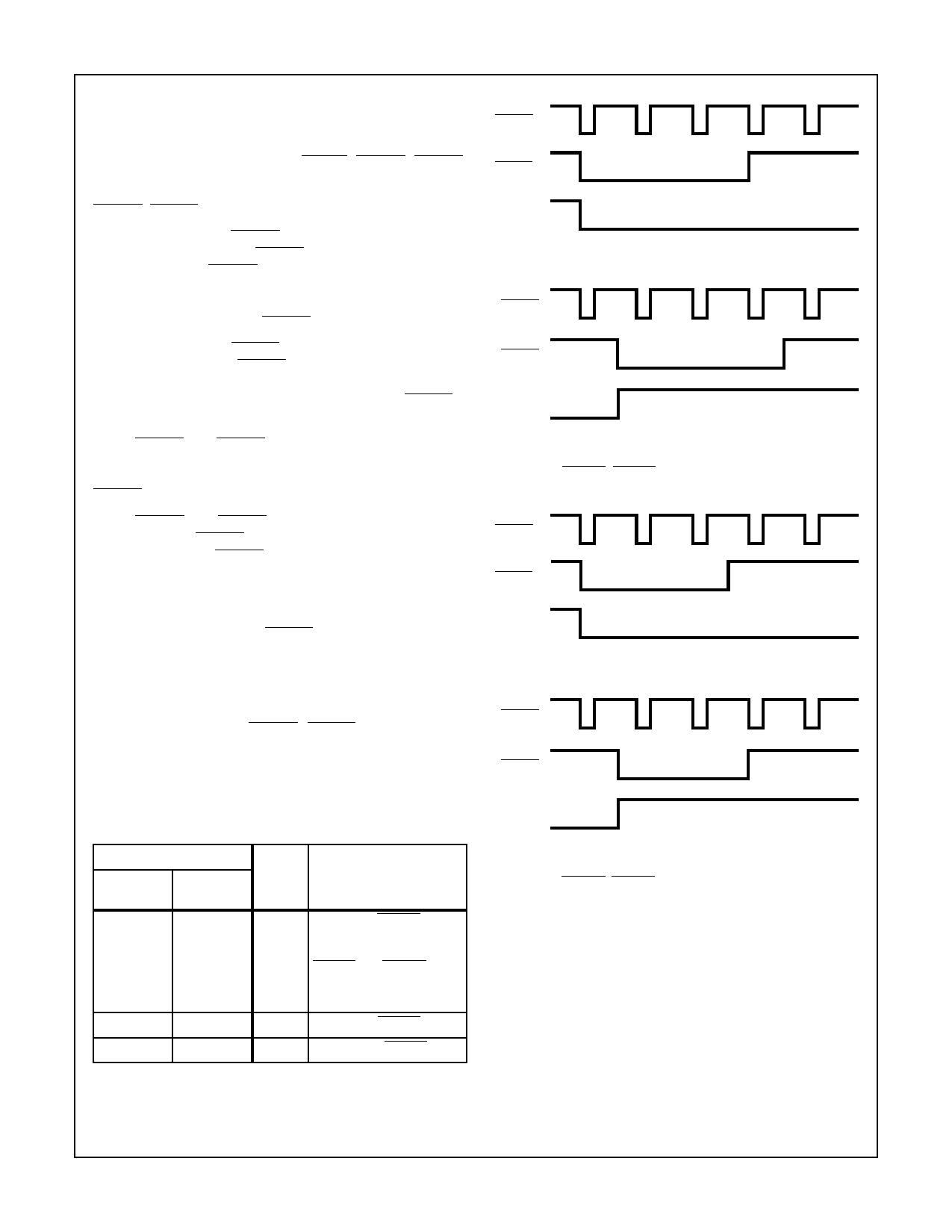
Figure 10 illustrates the HSYNC, VSYNC, and FIELD gen-
eral timing for (M, NSM) NTSC and (M, N) PAL. Figure 11
illustrates the general timing for (B, D, G, H, I, CN) PAL. In
the figures, all the signals are shown active low (their reset
state), and FIELD is low during odd fields.
TABLE 6. FIELD OUTPUT TIMING
FIELD
FIGURE 10A. BEGINNING AN ODD FIELD
HSYNC
VSYNC
FIELD
FIGURE 10B. BEGINNING AN EVEN FIELD
FIGURE 10. HSYNC, VSYNC, AND FIELD TIMING FOR
(M, NSM) NTSC AND (M, N) PAL
HSYNC
VSYNC
FIELD
FIGURE 11A. BEGINNING AN ODD FIELD
HSYNC
VSYNC
FIELD
OPERATING MODE
SYNC I/O BLANK I/O CLK2
DIRECTION DIRECTION DELAY
COMMENTS
Input
Input
148 FIELD lags VSYNC switch-
ing from odd to even.
FIELD lags the earlier of
VSYNC and HSYNC when
syncs are aligned when
switching from even to odd.
Input
Output
138 FIELD lags VSYNC.
Output Don’t Care 32 FIELD leads VSYNC.
FIGURE 11B. BEGINNING AN EVEN FIELD
FIGURE 11. HSYNC, VSYNC, AND FIELD TIMING FOR
(B, D, G, H, I, CN) PAL
10
Share Link: 