HMP8156 データシートの表示(PDF) - Intersil
部品番号
コンポーネント説明
メーカー
HMP8156 Datasheet PDF : 33 Pages
| |||
HMP8156
CLK2
CLK
P0-P15
OL0-OL2,
M1, M0
BLANK
(INPUT)
BLANK
(OUTPUT)
RGB 0
PIXEL 0
RGB 1
PIXEL 1
RGB N
PIXEL N
FIGURE 7. PIXEL AND OVERLAY INPUT TIMING - 16-BIT RGB WITH 2X UPSAMPLING
CLK2
CLK
P0-P24
BLANK
(INPUT)
BLANK
(OUTPUT)
RGB 0
RGB 1
RGB N
CLK2
FIGURE 8. PIXEL AND OVERLAY INPUT TIMING - 24-BIT RGB WITH 2X UPSAMPLING
P8-P15 Cb 2 Y 2
Cr 2
Y3
Cb 4
Y4
"FF" "00" "00" "XY" "10" "80" "10"
OL0-OL2,
M1, M0
PIXEL 0
PIXEL 1
PIXEL N-2
PIXEL N-1
PIXEL N
BLANK
(OUTPUT)
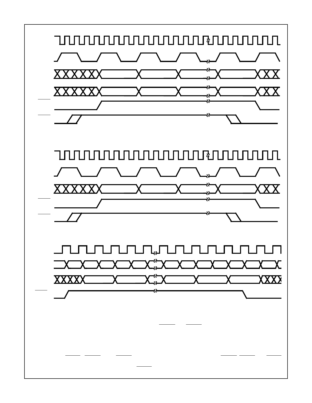
FIGURE 9. PIXEL AND OVERLAY INPUT TIMING - BT.656
8-Bit Parallel ITU-R BT.656 Format
When ITU-R BT.656 format is selected, data is latched on
each rising edge of CLK2. Overlay data is latched when the
Y input data is latched. However, the overlay data must
arrive three pixels after its corresponding Y data. The pixel
and overlay input timing is shown in Figure 9.
As inputs, the BLANK, HSYNC, and VSYNC pins are
ignored since all timing is derived from the EAV and SAV
sequences within the data stream. As outputs, BLANK,
HSYNC and VSYNC are output following the rising edge of
CLK2. If the CLK pin is configured as an input, it is ignored. If
configured as an output, it is one-half the CLK2 frequency.
Square pixel operation, overlay processing with internal mix-
ing, and SIF mode 2X upsampling are not supported for the
BT.656 input format. Also, the HSYNC, VSYNC, and BLANK
signals must be configured as outputs.
9
Share Link: 