74LVC245AD データシートの表示(PDF) - Philips Electronics
部品番号
コンポーネント説明
メーカー
74LVC245AD
74LVC245AD Datasheet PDF : 20 Pages
| |||

Philips Semiconductors
Product specification
Octal bus transceiver with direction pin with 5 V tolerant 74LVC245A;
input/outputs (3-state)
74LVCH245A
FEATURES
• 5 V tolerant inputs/outputs for interfacing with 5 V logic
• Wide supply voltage range from 1.2 to 3.6 V
• CMOS low power consumption
• Direct interface with TTL levels
• Inputs accept voltages up to 5.5 V
• High-impedance when VCC = 0 V
• bus-hold on all data inputs (74LVCH245A only)
• Complies with JEDEC standard no. 8-1A
• ESD protection:
HBM EIA/JESD22-A114-A exceeds 2000 V
MM EIA/JESD22-A115-A exceeds 200 V
• Specified from −40 to +85 °C and −40 to +125 °C.
DESCRIPTION
The 74LVC245A/74LVCH245A is a high-performance,
low-power, low-voltage, Si-gate CMOS device, superior to
most advanced CMOS compatible TTL families.
Inputs can be driven from either 3.3 or 5 V devices.
In 3-state operation outputs can handle 5 V. These
features allow the use of these devices as translators in a
mixed 3.3 and 5 V environment.
The 74LVC245A/74LVCH245A is an octal transceiver with
non-inverting 3-state bus compatible outputs in both send
and receive directions.
The 74LVC245A/74LVCH245A has an output enable (OE)
input for easy cascading and a send/receive (DIR) input for
direction control. OE controls the outputs so that the buses
are effectively isolated.
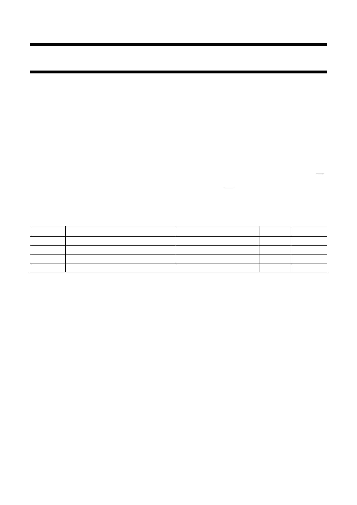
QUICK REFERENCE DATA
GND = 0 V; Tamb = 25 °C; tr = tf ≤ 2.5 ns.
SYMBOL
tPHL/tPLH
CI
CI/O
CPD
PARAMETER
propagation delay An to Bn, Bn to An
input capacitance
input/output capacitance
power dissipation capacitance per buffer
CONDITIONS
CL = 50 pF; VCC = 3.3 V
VCC = 3.3 V; notes 1 and 2
Notes
1. CPD is used to determine the dynamic power dissipation (PD in µW).
PD = CPD × VCC2 × fi × N + Σ(CL × VCC2 × fo) where:
fi = input frequency in MHz;
fo = output frequency in MHz;
CL = output load capacitance in pF;
VCC = supply voltage in Volts;
N = total load switching outputs;
Σ(CL × VCC2 × fo) = sum of the outputs.
2. The condition is VI = GND to VCC.
TYPICAL
2.9
4.0
10.0
15
UNIT
ns
pF
pF
pF
2003 May 07
2