LC74780(2001) データシートの表示(PDF) - SANYO -> Panasonic
部品番号
コンポーネント説明
メーカー
LC74780 Datasheet PDF : 14 Pages
| |||
Serial Data Input Timing
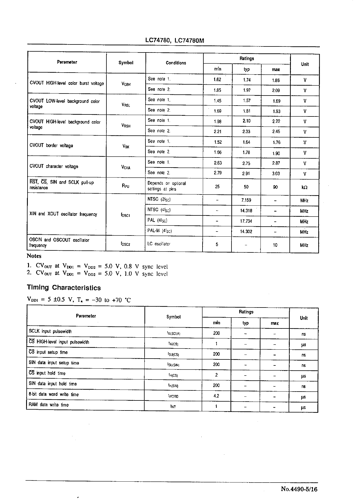
LC74780, 74780M
Display Control Features and Characteristics
Display Control Command Structure
The display control commands, COMMAND0 to COM-
MAND7, are shifted in 8-bit serial units. The first byte of a
command consists of an identification code and data. The
second byte consists of data only. Once the command iden-
tification code in byte 1 has been written, it is saved until
Display Control Command Data
the next time the first byte is written. If COMMAND1 is
written, the display character write mode begins and the
first byte does not change. When CS is HIGH, COM-
MAND0 is set.
Command
COMMAND0
Display memory (VRAM) write
address setting command
COMMAND1
Display character data write
command
COMMAND2
Vertical display position and
character size setting
command
COMMAND3
Horizontal display position and
character size setting
command
COMMAND4
Display control setting
command
COMMAND5
Display control setting
command
COMMAND6
Synchronization signal control
setting command
COMMAND7
Display control setting
command
First byte
Command code
Data or register storing data
7
6
5
4
3
2
1
0
7
1
0
0
0 V3 V2 V1 V0 0
Second byte
Data or register storing data
6
5
4
3
2
1
0
0
0 H4 H3 H2 H1 H0
1
0
0
1
0
0
0
0
at C6 C5 C4 C3 C2 C1 C0
1
0
1
0 VS21 VS20 VS11 VS10 0 FS VP5 VP4 VP3 VP2 VP1 VP0
1
0
1
1 HS21 HS20 HS11 HS10 0 LC HP5 HP4 HP3 HP2 HP1 HP0
1
1
0
0
TST RAM OSC SYS
MOD ERS STP RST
0
BLK2 BLK1 BLK0 BK1 BK0
RV
DSP
ON
1
1
0
1 NP1 NP0 NON INT 0
0
0 BCL CB PH2 PH1 PH0
1
1
1
0
MOD1 MOD0
DIS
LIN
MUT
0
RN2 RN1 RN0 SN3 SN2 SN1 SN0
1
1
1
1 EX1 PD1 EX0 PD0
No.4490–5/14
Share Link: 