AIC1803 データシートの表示(PDF) - Analog Intergrations
部品番号
コンポーネント説明
メーカー
AIC1803 Datasheet PDF : 12 Pages
| |||
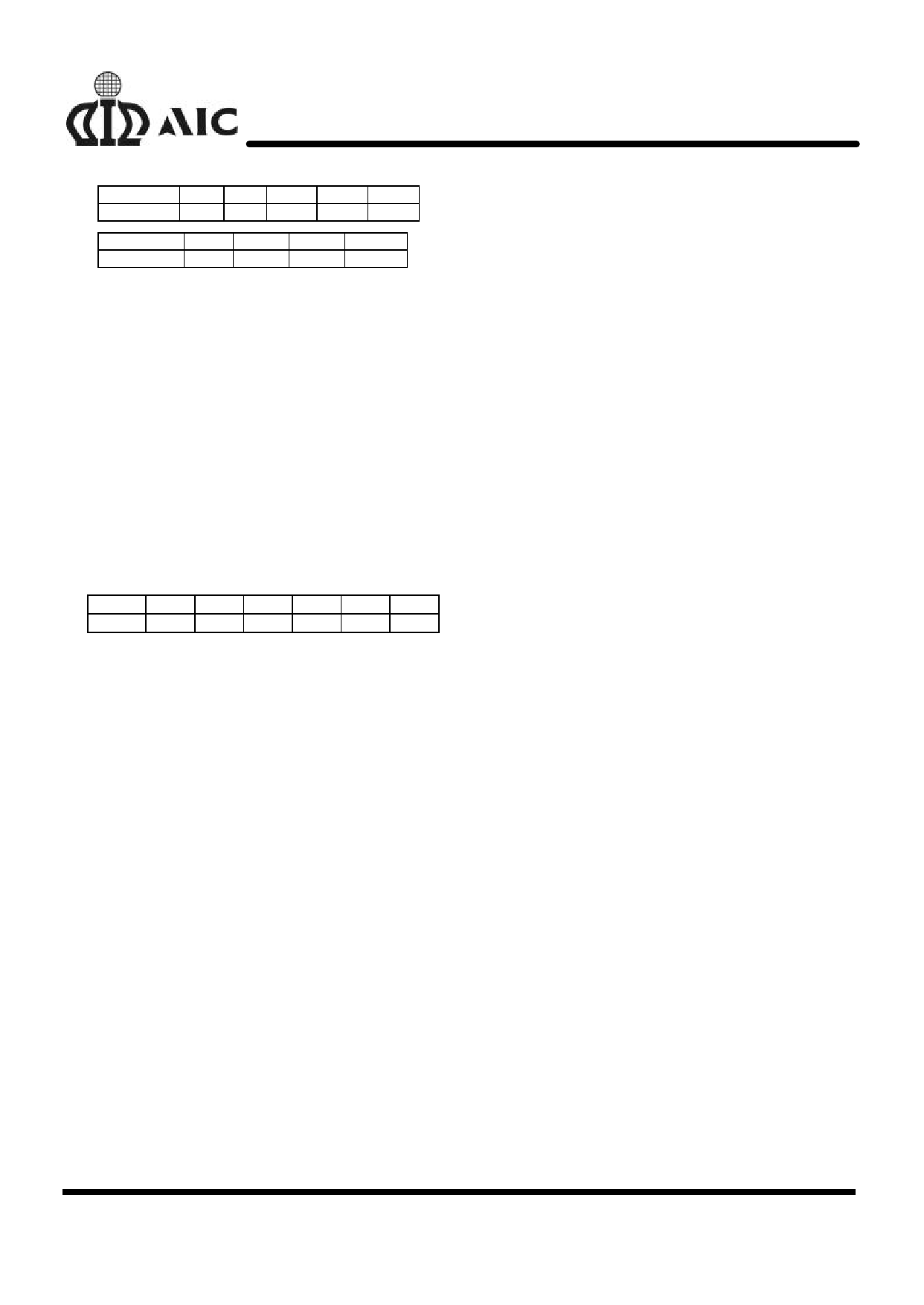
CTC ‚CTD(F)
TOC ‚TOD(S)
CTC ‚CTD(F)
TOC ‚TOD(S)
1n 5n 10n 22n 33n
21m 52m 132m 253m 347m
47n 68n 82n 100n
617m 748m 1004m 1630m
The delay time can also be approximately
calculated by the following equations (if CTC , CTD
≤ 82nF) :
TOC(mS) = 11.8 x CTC(nF)
TOD(mS) = 11.8 x CTD(nF)
Setting the Overcurrent Delay Time 1
The overcurrent delay time 1 (TOI1) at 0.15V <
- VCC VCS < 0.3V is set by the external capacitor CTI,
while the overcurrent delay time 2 and 3 (TOI2 and
TOI3) is fixed by IC internal circuit.The relationship
between capacitance of the external capacitor and
delay time is tabulated as below.
CTI(F) 1n 2.2n 3.3n 5n
TOI(mS) 4.8 15.0 18.8 23.6
6.8n
31.0
10n
61.8
Selection of External Control
MOSFETs
Because the overcurrent protection voltage is
preset, the threshold current for overcurrent
detection is determined by the turn-on resistance
of the discharge control MOSFET M1. The turn-on
resistance of the external control MOSFETs can
be determined by the equation: RON=VOIP/IT (IT is
the overcurrent threshold current). For example, if
the overcurrent threshold current IT is designed to
be 5A, the turn-on resistance of the external
control MOSFETs must be 30mΩ. Users should
AIC1803
be aware that turn-on resistance of the MOSFET
changes with temperature variation due to heat
dissipation. It changes with the voltage between
gate and source as well. (Turn-on resistance of a
MOSFET increases as the voltage between gate
and source decreases). Once the turn-on
resistance of the external MOSFET changes, the
overcurrent threshold current will change
accordingly.
Suppressing the Ripple and
Disturbance from Charger
To suppress the ripple and disturbance from
charger, connecting R1 to R4 and C1 to C4 is
recommended.
Controlling the Charge Control
MOSFET
R5, R6, R7 and NPN transistor Q1 are used to
switch the charge control MOSFET M2. If
overcharge does not occur, no current flows into
OC pin and Q1 is turned off, then M2 is turned on.
When overcharge occurs, current flows into OC
pin and Q1 is turned on, which turns off M2 in turn.
Protection at CS Pin
R8 is used for protection of IC when charger is
connected in reverse. The charge detection
function after overdischarge is possibly disabled
by larger value of R8. Resistance of 1KΩ is
recommended.
10
Share Link: 