AIC1802 データシートの表示(PDF) - Analog Intergrations
部品番号
コンポーネント説明
メーカー
AIC1802 Datasheet PDF : 10 Pages
| |||
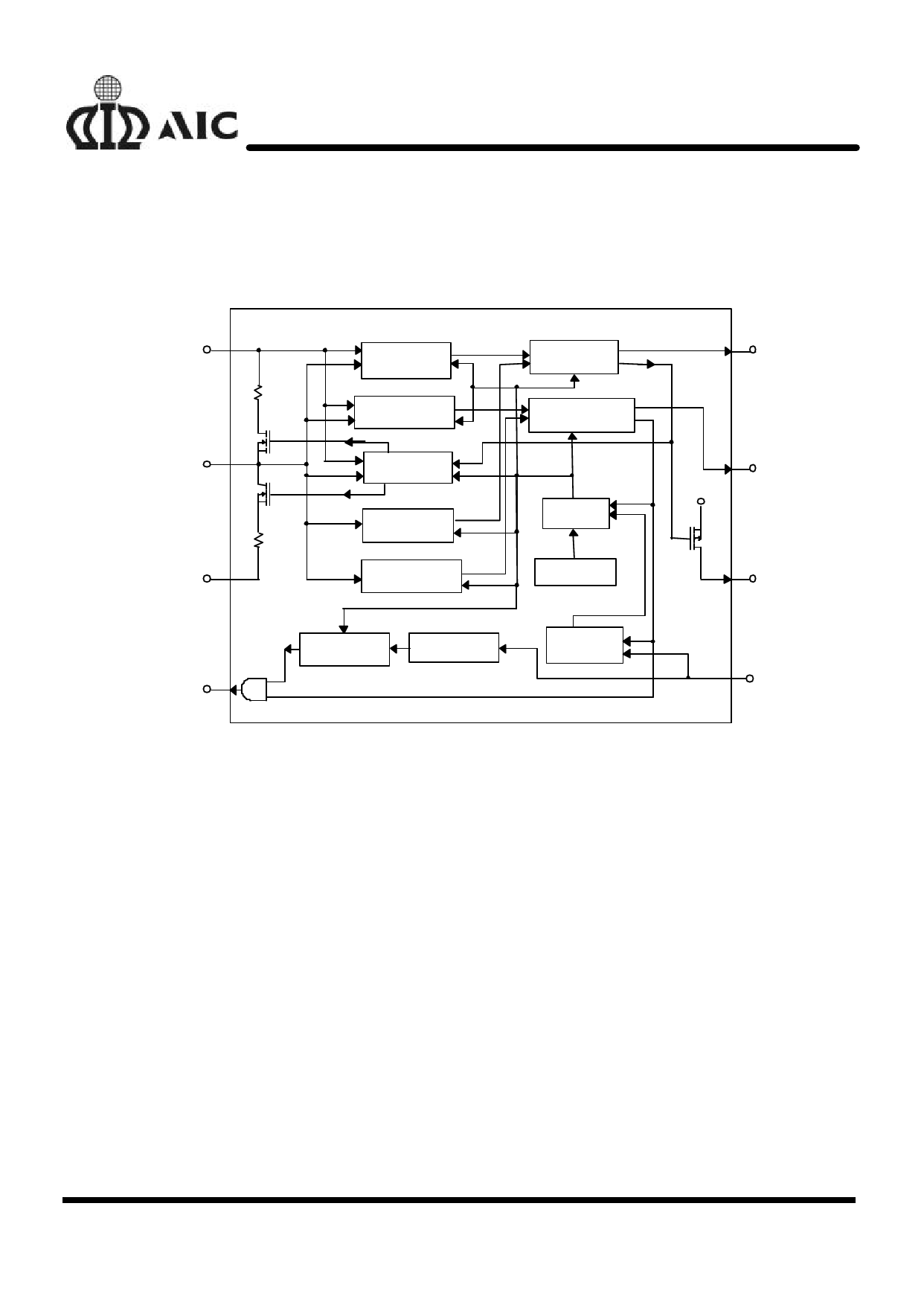
n BLOCK DIAGRAM
AIC1802
VCC 8
450
VC 6
450
GND 4
OVERCHARGE
DETECTOR 1
OVERDISCHARGE
DETECTOR 1
UNBALANCE
DISCHARGE
OVERCHARGE
DETECTOR 2
OVERDISCHARGE
DETECTOR 2
OVERCHARGE
DELAY CIRCUIT
5
TC
OVERDISCHARGE
DELAY CIRCUIT
POWER-
DOWN
LOGIC
CONTROL
WAKE-
UP
TIMING
GENERATION
3
TD
VCC
1
OC
OD 2
OVERCURRENT
DELAY CIRCUIT
OVERCURRENT
DETECTOR
CHARGE
DETECTION
7 CS
n PIN DESCRIPTIONS
PIN 1: OC
- PMOS open drain output for
control of the charge control
MOSFET M2. When overcharge
occurs, this pin sources current to
switch the external NPN Q1 on,
and charging is inhibited by
turning off the charge control
MOSFET M2.
PIN 2: OD
- Output pin for control of the
discharge control MOSFET M1.
When overdischarge occurs, this
pin goes low to turn off the
discharge control MOSFET M1
and discharging is inhibited.
PIN 3: TD - Overdischarge delay time setting
pin.
PIN 4: GND - Ground pin. This pin is to be
connected to the negative terminal
of the lower battery cell.
PIN 5: TC - Overcharge delay time setting
pin.
PIN 6: VC
- To be connected to the positive
terminal of the lower cell and
the negative terminal of the
upper cell.
PIN 7: CS
- Input pin for current sensing.
Using the drain-source voltage
of the discharge control
MOSFET M1 (voltage between
CS and GND), it senses
discharge current during normal
mode and detects whether
charging current is present
during power down mode.
PIN 8: VCC - Power supply pin. It is to be
connected to the positive
terminal of the upper cell.
6
Share Link: 