HT9480(1998) データシートの表示(PDF) - Holtek Semiconductor
部品番号
コンポーネント説明
メーカー
HT9480 Datasheet PDF : 57 Pages
| |||
HT9480
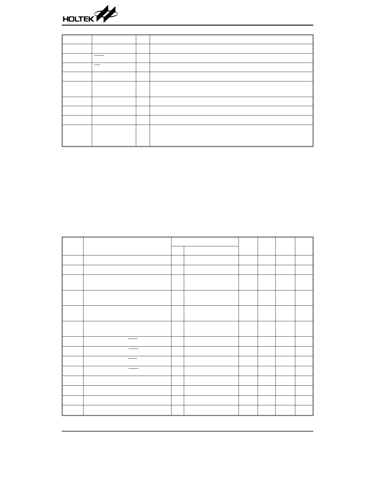
Pin Description
Pin No
43~49
54~61
62~63
1, 42,
52, 64
76
77
40
41
53
68
50
2, 39, 51
67
65
3~34
78~80
35~38
66
75
69
70
71
72
73
74
Pin Name
PA0~PA6
PB0~PB7
PC0~PC1
I/O
Function
I
7-bit input ports, with pull-high resistors
Each bit can be configured as a wake-up input by mask option.
Bidirectional 8-bit input/output ports, pull-high mask option
I/O The output structures, whether tri-state or CMOS, are
determined by software instructions.
Bidirectional 2-bit input/output ports, pull-high mask option
I/O The output structures, whether tri-state or CMOS, are
determined by software instructions.
VSS
Negative power supply (GND)
X1
X2
OSC1
OSC2
RES
BAF
TMR1
I X1 and X2 are connected to an external crystal to form an
O internal low power oscillator clock.
OSC1 and OSC2 are connected to an RC network or a crystal
I (determined by mask option) to form the system clock oscillator.
O For RC operation, OSC2 is the output terminal of the system
clock.
I Schmitt trigger reset input, active low
I Battery fail interrupt with debounce circuit input
I Schmitt trigger input for timer/event counter
VDD
Positive power supply
Buzzer non-inverting BZ output
BZ
O The BZ pin outputs “high” at buzzer off (by setting the value 00H
of 1DH)
SEG31~SEG0
SEG34~SEG32
O LCD driver outputs for LCD panel segments
COM3~COM0 O Outputs for LCD panel common connections
TSC
I µC test mode input pin, active low with pull-high resistor
TS
I Decoder test mode input pin, active low with a pull-high resistor
BAL
I
Battery low indication input, active high without pull-high
resistor
DI
I
POCSAG code input serial data (inverting or non-inverting as
determined by SPF32). CMOS input without pull-high resistor
BS1
O Pager receiver power control enable output, CMOS output
BS2
O RF dc level adjustment pin, CMOS output
BS3
O PLL control pin, CMOS output
FOUT
Frequency reference output pin
O The FOUT output pin produces a 76.8kHz/153.6kHz signal with
a 1/2 duty cycle reference frequency if a 76.8kHz crystal is used.
4
23th Feb ’98
Share Link: 