UAA3500HL データシートの表示(PDF) - Philips Electronics
部品番号
コンポーネント説明
メーカー
UAA3500HL Datasheet PDF : 16 Pages
| |||
Philips Semiconductors
Pager receiver
Preliminary specification
UAA3500HL
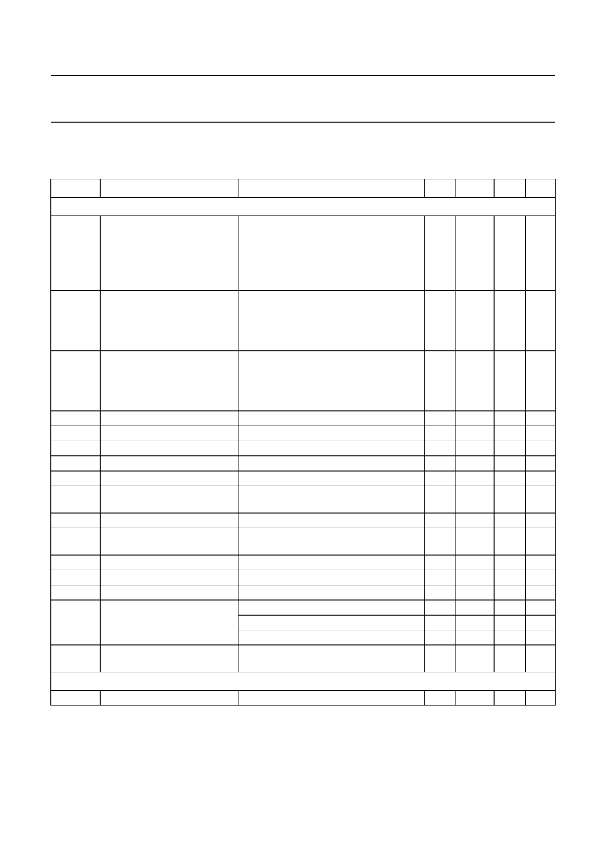
AC CHARACTERISTICS
VCC = 2.1 V; Tamb = 25 °C; 930 MHz band application, 3% BER and 1600 bits/s 2 level; on evaluation board according
to Fig.3; system measurement done using PCD5009, PCD5010 baseband; unless otherwise specified.
SYMBOL
PARAMETER
CONDITIONS
MIN. TYP. MAX. UNIT
Receiver
Pi(ref)
RF input sensitivity
G(PCFE)
front-end conversion power
gain
NFRX
receiver noise figure
IP1
IP2
IP3
IM3
CCR
ACR
αbl
GAGC
AGCth
ton
∆IQ
RLNA
1 dB input compression point
2nd order intercept point
3rd order intercept point
3rd order intermodulation
co-channel rejection
adjacent channel rejection
blocking immunity
front-end gain reduction by
AGC step
AGC threshold
establishment time
IQ channel unbalance
LNA current set resistor
Rgyr
gyrator cut-off frequency set
resistor
3% BER
fRF = 160 MHz; 1600 bits/s 2-level FSK −
fRF = 280 MHz; 1600 bits/s 2-level FSK −
fRF = 930 MHz; 6400 bits/s 2-level FSK −
fRF = 930 MHz; 6400 bits/s 4-level FSK −
from RF input to 2nd mixer input
fRF = 160 MHz
−
fRF = 280 MHz
−
fRF = 930 MHz
−
from RF input to 2nd mixer input
fRF = 160 MHz
−
fRF = 280 MHz
−
fRF = 930 MHz
−
from RF input to 2nd mixer input
−
from 2nd mixer input to gyrator output
45
from RF input to 2nd mixer input; note 1 −
3 signal measurement
55
threshold +3 dB
−
channel spacing = 25 kHz; from RF input 65
to gyrator output
frequency offset >1 MHz
75
7
above sensitivity
20
until sensitivity +3 dB is reached
−
−
160 MHz
−
280 MHz
−
930 MHz
−
cut-off frequency = 8.5 kHz
−
−128.5 −
−128 −
−126.5 −
−123 −
20
−
12.8 −
12.7 −
2.7
−
3.1
−
4.4
−
−38 −
−
−
−33 −
−
−
5
−
70
−
80
−
8
9
25
30
−
30
−
2
56
−
47
−
27
−
47
−
dBm
dBm
dBm
dBm
dB
dB
dB
dB
dB
dB
dBm
dBm
dBm
dB
dB
dB
dB
dB
dB
ms
dB
kΩ
kΩ
kΩ
kΩ
LO
fVCO
VCO frequency
−
2⁄3fRF −
MHz
2000 Jan 18
10
Share Link: 