UAA3500HL データシートの表示(PDF) - Philips Electronics
部品番号
コンポーネント説明
メーカー
UAA3500HL Datasheet PDF : 16 Pages
| |||
Philips Semiconductors
Pager receiver
Preliminary specification
UAA3500HL
FUNCTIONAL DESCRIPTION
Receiver front-end section
The receiver front-end consists of an LNA, followed by the
first and the second mixers. For operation at low frequency
(160 and 280 MHz, for instance), the first mixer can be
bypassed, saving some current. The image rejection is
done by an external LC filter placed between the LNA, the
first mixer and the antenna selectivity. The IF band is
filtered by an external filter placed between the first mixer
and the second mixers for the I and Q paths. The
RF signals are in phase, and the LO signals are shifted
by 90°. The output signals are at zero frequency.
To increase the immunity to interferers, an AGC loop
controls the LNA gain by attenuating the RF input signal.
Four steps of attenuation are possible (each having 8 dB),
ranging therefore from 0 to 32 dB. The AGC loop
threshold level and time constant may be controlled
externally at pins AGCADJ and AGCTAU. The second
LO I/Q phase shift is made by a quadrature divider, whose
input is the VCO oscillating signal.
The LNA current is setup by an external resistor. All the
receivers (front-end and back-end) are turned on by
pin RXON.
Receiver back-end section
The down-converted signal is amplified and then filtered
by a Sallen-Key filter, which shows a notch at 15 kHz and
about 6 dB rejection out-of-band. Then comes the first
high-pass filter (DC block), followed by the gyrator filter,
which performs an elliptic, 7-pole low-pass filtering. The
signal is then amplified by the first limiter, filtered by the
second DC block, amplified again, and filtered again by
the third DC block. Finally, an output stage delivers the
signal with rail-to-rail logic levels.
The first, second and third DC block frequencies are set at
4, 8 and 12 Hz respectively by external 330 nF capacitors.
The two voltage regulators are also activated by RXON.
At the output of the gyrator filter, the signal is buffered and
logarithmically converted. It then controls the AGC loop.
To rapidly reach the DC operating point, a fast mode is
built into the three DC blocks.
LO
The external VCO is AC-coupled at input LOIN. It is then
buffered to drive the first mixer. LOIN also enters a
quadrature divider-by-2, whose output signals are also
buffered to drive the second mixers. The VCO frequency
should be 2⁄3 of the input RF signal.
The LO signal must be generated with an external
frequency synthesizer and VCO or with a crystal oscillator.
OPERATING MODES
To use the IC, all VCC pins must be connected to the
supply voltage B++ (2.1 V). The 1.8 V regulated voltage
sinks current from B++ and the 1.0 V regulated voltage
from B+ (1.4 V). In a typical application, the B+ supply is
the battery and the B++ supply is the DC/DC converter
located in the baseband chip.
In normal operating mode, the receiver should be
powered-on in fast mode. The fast mode can be turned off
after several milliseconds.
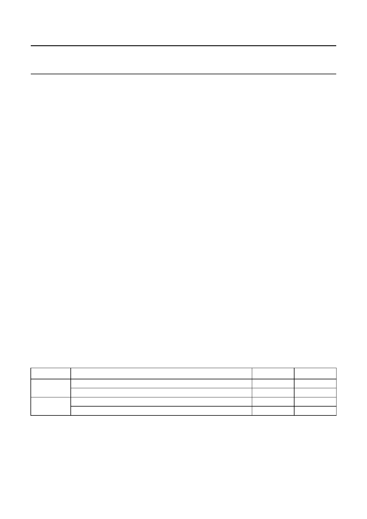
Table 1 gives the definition of the polarity of the switching
signals on the receive section.
Table 1 Switching signals on the receiver
SIGNAL
RXON
FASTON
SECTION
receive section powered-on
receive section powered-off
fast mode powered-on
fast mode powered-off
LEVEL
HIGH
LOW
HIGH
LOW
ON/OFF
on
off
on
off
2000 Jan 18
7
Share Link: 