M28C64C データシートの表示(PDF) - STMicroelectronics
部品番号
コンポーネント説明
メーカー
M28C64C Datasheet PDF : 15 Pages
| |||
M28C64C, M28C64X
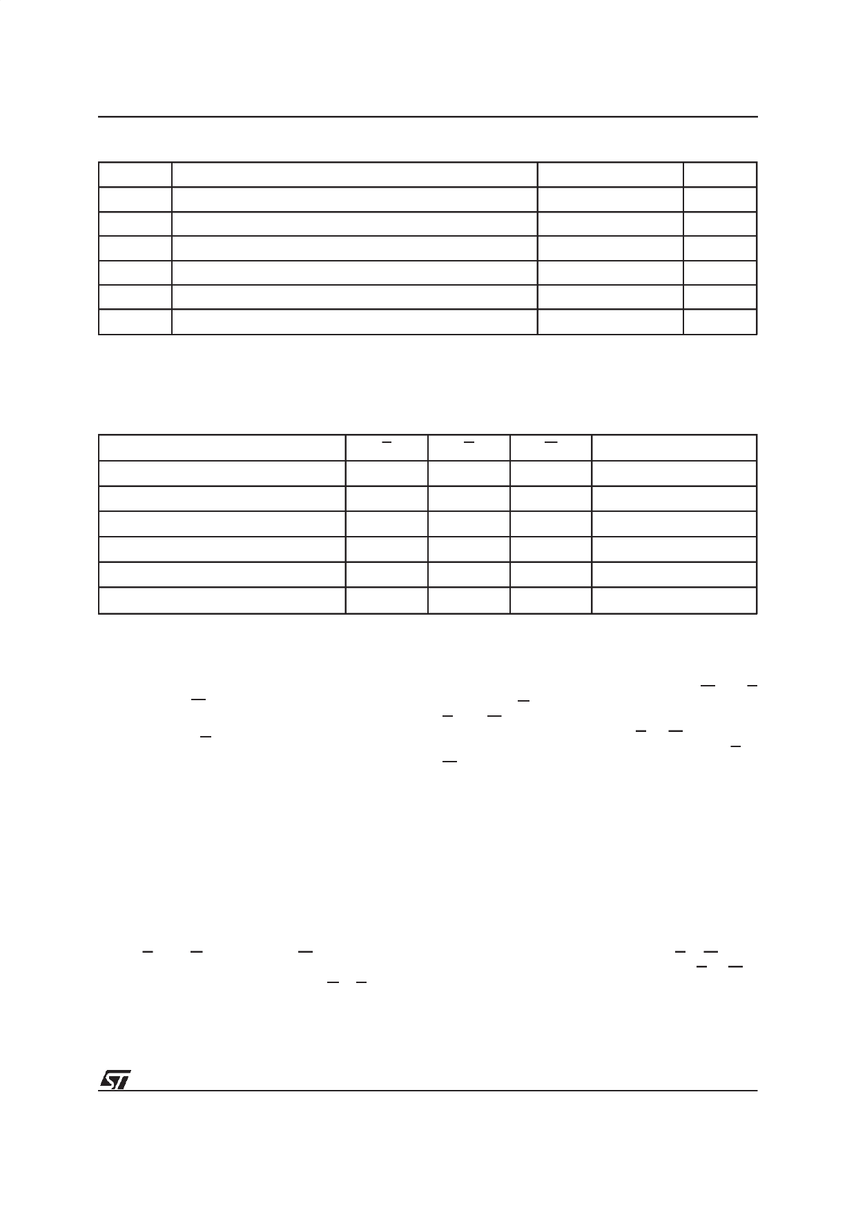
Table 2. Absolute Maximum Ratings
Symbol
Parameter
Value
Unit
TA
Ambient Operating Temperature
– 40 to 125
°C
T STG
Storage Temperature Range
– 65 to 150
°C
VCC
Supply Voltage
– 0.3 to 6.5
V
VIO
Input/Output Voltage
– 0.3 to VCC +0.6
V
VI
Input Voltage
– 0.3 to 6.5
V
VESD Electrostatic Discharge Voltage (Human Body model)
2000
V
Note: Except for the rating ”Operating Temperature Range”, stresses above those listed in the Table ”Absolute Maximum Ratings” may
cause permanent damage to the device. These are stress ratings only and operation of the device at these or any other conditions above
those indicated in the Operating sections of this specification is not implied. Exposure to Absolute Maximum Rating conditions for extended
periods may affect device reliability. Refer also to the STMicroelectronics SURE Program and other relevant quality documents.
Table 3. Operating Modes
Mode
Read
Write
Standby / Write Inhibit
Write Inhibit
Write Inhibit
Output Disable
Note: X = VIH or VIL
E
G
W
VIL
VIL
VIH
VIL
VIH
VIL
VIH
X
X
X
X
VIH
X
VIL
X
X
VIH
X
DQ0 - DQ7
Data Out
Data In
Hi-Z
Data Out or Hi-Z
Data Out or Hi-Z
Hi-Z
Data In/ Out (DQ0 - DQ7). Data is written to or read
from the M28C64C through the I/O pins.
Write Enable (W). The Write Enable input controls
the writing of data to the M28C64C.
Ready/Busy (RB). Ready/Busy is an open drain
output that can be used to detect the end of the
internal write cycle.
OPERATION
In order to prevent data corruption and inadvertent
write operations during power-up, a Power On
Reset (POR) circuit resets all internal programming
cicuitry. Access to the memory in write mode is
allowed after a power-up as specified in Table 6.
Read
The M28C64C is accessed like a static RAM.
When E and G are low with W high, the data
addressed is presented on the I/O pins. The I/O
pins are high impedancewhen either G or E is high.
Write
Write operations are initiated when both W and E
are low and G is high.The M28C64C supports both
E and W controlled write cycles. The Address is
latched by the falling edge of E or W which ever
occurs last and the Data on the rising edge of E or
W which ever occurs first. Once initiated the write
operation is internally timed until completion.
Page Write
Page write allows up to 32 bytes to be consecu-
tively latched into the memory prior to initiating a
programming cycle. All bytes must be located in a
single page address, that is A5 - A12 must be the
same for all bytes. The page write can be initiated
during any byte write operation.
Following the first byte write instruction the host
may send another address and data up to a maxi-
mum of 100µs after the rising edge of E or W which
ever occurs first (tBLC). If a transition of E or W is
not detected within 100µs, the internal program-
ming cycle will start.
3/15
Share Link: 