RF2146 データシートの表示(PDF) - RF Micro Devices
部品番号
コンポーネント説明
メーカー
RF2146 Datasheet PDF : 8 Pages
| |||
RF2146
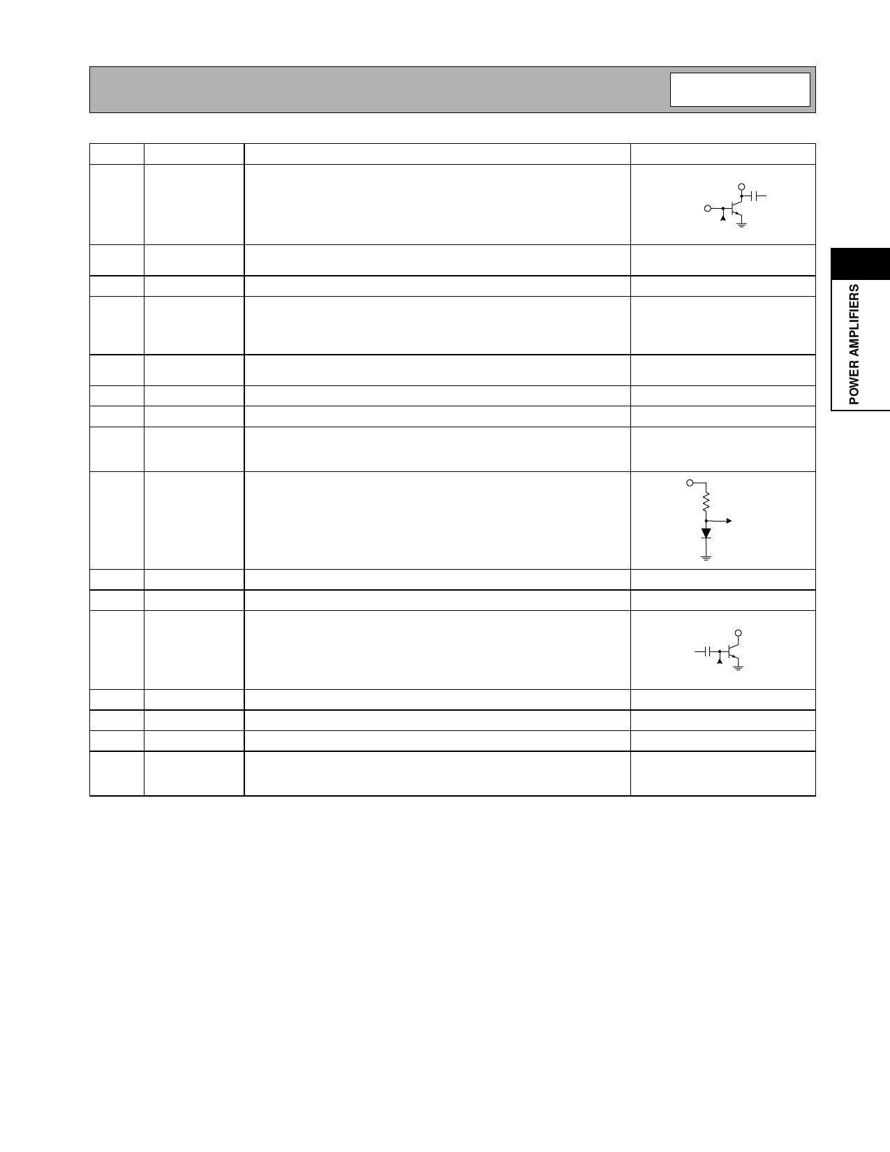
Pin Function Description
Interface Schematic
1
VCC
Power supply for the driver stage, and interstage matching. Shunt
VCC
capacitance is required on this pin. The value of the capacitance is fre-
quency dependent. 4.7pF centers the gain at 1880 MHz.
RF IN
From Bias
Stages
2
GND
Ground connection for final stage. Keep traces physically short and
connect immediately to the ground plane for best performance.
2
3
GND
Same as pin 2.
4
RF IN
RF input. This is a 50Ω input, but the actual input impedance depends See pin 1.
on the interstage matching network connected to pin 1. An external DC
blocking capacitor is required if this port is connected to a DC path to
ground or a DC voltage.
5
GND
Ground connection for the driver stage. Keep traces physically short
and connect immediately to the ground plane for best performance.
6
GND
Same as pin 2.
7
GND
Same as pin 2.
8
BYP1
Bypass Pin. Part of the matching circuit for interstage match. DC con- See pin 1.
nected to VCC1. Use a suitable bypass capacitor to ground. Keep
capacitor as close to pin as possible.
9
PC
Power Control. When this pin is "low", all circuits are shut off. A "low" is
PC
typically 0.5V. When this pin is "high", the part operates normally, and
the pin consumes approximately 13mA during normal operation.
This pin should never exceed 5V.
To RF
Transistors
10
GND
Same as pin 2.
11
GND
Same as pin 2.
12
RF OUT RF Output and power supply for the output stage. The two output pins
are combined, and bias voltage for the final stage is provided through
these pins. An external matching network is required to provide the
optimum load impedance; see the application schematics for details.
RF OUT
From Bias
Stages
13
RF OUT Same as pin 12.
See pin 12.
14
GND
Same as pin 2.
15
GND
Same as pin 2.
16
BYP2
Bypass Pin. Part of the matching circuit for interstage match. DC con- See pin 1.
nected to VCC1. For 1880 MHz operation, use a 3.3pF capacitor to
ground. Keep capacitor as close to pin as possible.
Rev A3 001026
2-149
Share Link: 