HS7541A データシートの表示(PDF) - Signal Processing Technologies
部品番号
コンポーネント説明
メーカー
HS7541A Datasheet PDF : 7 Pages
| |||
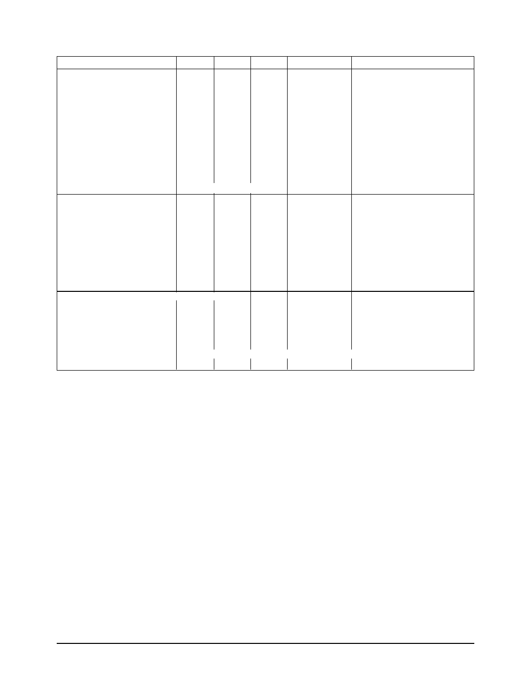
SPECIFICATIONS (continued)
(TA=25°C; VDD =+15V, VREF = +10V; IO1 = IO2 = GND = 0V; unipolar unless otherwise noted.)
PARAMETER
MIN. TYP. MAX.
UNIT
CONDITIONS
DIGITAL INPUTS
Logic Levels
VIH
VIL
Input Current
Input Capacitance
Bits 1—12
Coding
Unipolar
Bipolar
2.4
VDD
2.4
-0.3
0.8
0.8
±1.0
±10
8
Binary
Offset Binary
Volts
Volts
Volts
Volts
µA
µA
pF
Note 5
Note 5
VIN = 0V or VDD
Note 5 and 15
VIN = 0; Note 5 and 14
Note 5
POWER REQUIREMENTS
Voltage Range
Supply Current
+5
+15
+16
2.0
2.5
2.5
0.2
0.5
1.0
ENVIRONMENTAL AND MECHANICAL
Volts
Volts
mA
mA
mA
mA
Note 16
Note 5
All digital inputs VIL or VIH
Note 5; all digital inputs VIL or
VIH
All digital inputs 0V or 5V to
VDD
Note 5; all digital inputs 0V or
5V to VDD
Operating Temperature
-AK, -AJ
-AB, -AA
Storage Temperature
Package
-AK, -AJ
0
+70
°C
-40
+85
°C
-65
+150
°C
18-pin plastic DIP, 20-pin PLCC, 18–pin SOIC
Notes and Cautions:
1.
Do not apply voltages higher than VDD or less than GND potential on any terminal other than VREF or VRFB.
2.
The digital inputs are diode-clamp protected against ESD damage. However, permanent damage may occur
on unprotected units from high-energy electrostatic fields. Keep units in conductive foam at all times until
ready to use.
3.
Use proper anti-static handling procedures.
4.
Stresses above those listed under “Absolute Maximum Ratings” may cause permanent damage to the
device. This is a stress rating only and functional operation at or above these specifications is not implied.
Exposure to the above maximum rated conditions for extended periods may affect device reliability.
5.
From TMIN to TMAX.
6.
Integral Non-linearity is measured as the arithmetic mean value of the magnitudes of the greatest positive
deviation and the greatest negative deviation from the theoretical value of any given input combination.
7.
Differential Non-linearity is the deviation of an output step from the theoretical value of 1 LSB for any two
adjacent digital input codes.
8.
AC performance characteristics are included for design guidance only and are subject to sample testing only.
9.
RL = 100Ω, CEXT = 13pF; all data inputs 0V to VDD or VDD to 0V; from 50% digital input change to 90% of final
analog output.
10.
Settling to ±0.01% FSR (strobed); all data inputs 0V to VDD or VDD to 0V.
11.
VREF = 0V, DAC register alternatively loaded with all 0’s and all 1’s.
12.
VREF = 20VP-P; F = 10kHz sinewave.
13.
VREF = 20VP-P; F = 1kHz sinewave.
14.
Guaranteed by design, but not production tested.
15.
Logic inputs are MOS gates. IIN typically is less than 1nA @ 25°C.
16.
Accuracy is guaranteed at VDD = +15V only.
17.
Measured using internal feedback resistor with DAC loaded with all 1’s.
18.
All digital inputs = 0V.
HS7541A
12-Bit CMOS Multiplying DAC
3
© Copyright 2000 Sipex Corporation
Share Link: 