LB1875 データシートの表示(PDF) - SANYO -> Panasonic
部品番号
コンポーネント説明
メーカー
LB1875 Datasheet PDF : 17 Pages
| |||
LB1875
4. Reference clock
Since the clock input of the PLL circuit (CLK ) and the internal divisor output (CLK ) are separate, various applications are
IN
OUT
possible.
(1) Using the internal divider circuit
Basically, CLKIN and CLKOUT are shorted. If a division ratio other than the built-in ratio is required, an external divider circuit can be
inserted between these two pins.
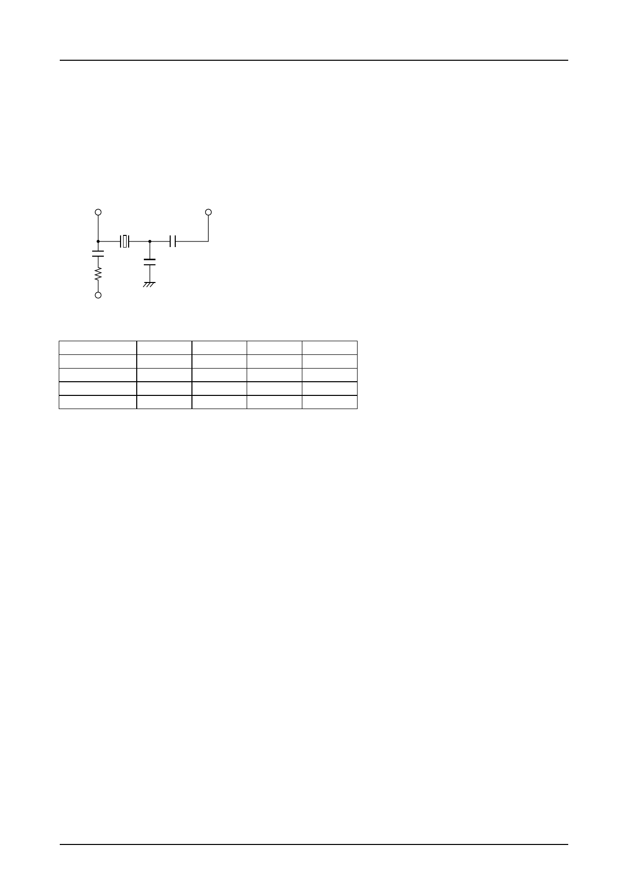
[1] Using a quartz oscillator
An oscillator using a quartz crystal and C, R components can be configured as shown below.
XI
C1
R1
XO
C3
C2
C1, R1 : For stable oscillation
C2 : For overtone oscillation prevention
C3 : For crystal coupling
VREG
(Reference values)
Oscillator frequency (MHz)
2 to 3
3 to 7
7 to 9
9 to 10
C1 (µF)
0.1
0.1
0.1
0.1
A11349
C2 (pF)
10
None
None
None
C3 (pF)
100
47
22
12
R1 ( Ω)
330k
330k
330k
330k
The circuit configuration and values are for reference only. The quartz crystal characteristics as well as the possibility of floating
capacitance and noise due to layout factors must be taken into consideration when designing an actual application.
[Precautions for wiring layout design]
Since the quartz oscillator circuit operates at high frequencies, it is susceptible to the influence of floating capacitance from the
circuit board. Wiring should be kept as short as possible and traces should be kept narrow.
[2] External clock input (equivalent to quartz oscillator, several MHz)
When using an external signal source instead of a quartz oscillator, a resistor of about 13 kΩ should be inserted in series at the XI
input. The XO pin should be left open.
Signal input level
Low: 0 to 0.8 V
High: 2.5 to 5 V
(2) When not using the internal divider circuit
When using an external signal source to supply a signal equivalent to the FG frequency (several kHz), the signal is input via the
CLKIN pin. When not using a quartz oscillator, the XI pin should be left open or connected to the VREG pin (XO is open).
5. Hall input signal
The Hall input requires a signal with an amplitude of at least the hysteresis width (24 mV max.). Taking possible noise influences
into consideration, an amplitude of at least 100 mV is desirable. If noise at the Hall input is a problem, a noise-canceling capacitor
(about 0.001 to 0.1 µF) should be connected across the Hall input pins .
Since the same-phase input range is 0 to V –2V, a Hall element can be connected in series if 12V is applied at the V pin.
CC
CC
6. FG input signal
The FG input is designed mainly for input from a Hall element and has the same specifications as the Hall input. If the input is to be
used for an FG pattern or other very low-level signal, an external amplifier must be used to amplify the signal first.
When there is noise at the FG input, locking may be impaired and jitter may increase. If PWM switching noise or other noise is found
to be present, countermeasures such as making the Hall element power supply more stable or connecting a capacitor across the input
will be necessary.
No. 6002-10/17
Share Link: 