ML4880CS データシートの表示(PDF) - Micro Linear Corporation
部品番号
コンポーネント説明
メーカー
ML4880CS Datasheet PDF : 15 Pages
| |||
The oscillator/one shot block generates a constant ON-
time and a minimum OFF-time. The OFF-time is extended
for as long as the output of the current comparator stays
low. Note that the inductor current flows in the current
sense resistor during the OFF-time. Therefore, a minimum
OFF-time is required to allow for the finite circuit delays
in sensing the inductor current. The ON-time is triggered
when the current comparator’s output goes high.
However, unlike conventional fixed ON-time controllers,
the ML4880’s one shot has an inverse relationship with
the input voltage as shown in Figure 4. Figure 5 plots the
inductor voltage-ON-time product. Note that the volt-
second product is nearly constant at voltages above 7V
input. This results in an inductor current ripple of:
∆IL
=
TON
× (VIN
L
−
VOUT )
(1)
It is important to note that the ripple current does not vary
in proportion with VIN, but remains nearly constant over a
wide input voltage range.
The transconductance amplifier generates a current from
the voltage difference between the reference and the
feedback voltage, VFB. This current produces a voltage
across Rgm that adds to the negative voltage that is
developed across the current sense resistor. When the
current level in the inductor drops low enough (a less
negative sense voltage) to cause the voltage at the non-
inverting input of the current comparator to go positive,
the comparator trips and starts a new ON cycle. In other
words, the current programming comparator controls the
length of the OFF-time by waiting until the inductor
current decreases to a value determined by the
transconductance amplifier.
This technique allows the feedback transconductance
amplifier’s output current to steer the current level in the
inductor. The higher the transconductance amplifier’s
output current, the higher the inductor current. For
example, when the output voltage drops due to a load
increase, the transconductance amplifier will increase its
output current and generate a larger voltage across Rgm,
ML4880
which in turn raises the inductor current trip level,
shortening the OFF-time. At some level of increasing the
output load, the transconductance amplifier can no longer
continue to increase its output current. When this occurs,
the voltage across Rgm reaches a maximum and the
inductor current cannot increase. If the inductor current
tries to increase, the voltage developed across the current
sense resistor would become more negative, causing the
non-inverting input of the current comparator to be
negative, which extends the OFF-time and reduces the
inductor current.
When the output voltage is too high, the
transconductance amplifier’s output current will
eventually become negative. However, since the inductor
current flows in only one direction (assuming no shoot
through current) the non-inverting input of the current
comparator will also stay negative. This extends the OFF-
time allowing the inductor current to decrease to zero and
causing the converter to stop operation until the output
voltage drops enough to increase the output current of the
transconductance amp above zero.
In summary, the three operation modes can be defined by
the voltage at the ISENSE pin at the end of the OFF-time:
VSENSE ≥ 0V
Discontinuous
current mode
0V > VSENSE > –140mV
Continuous
current mode
–140mV > VSENSE > –250mV Current limit
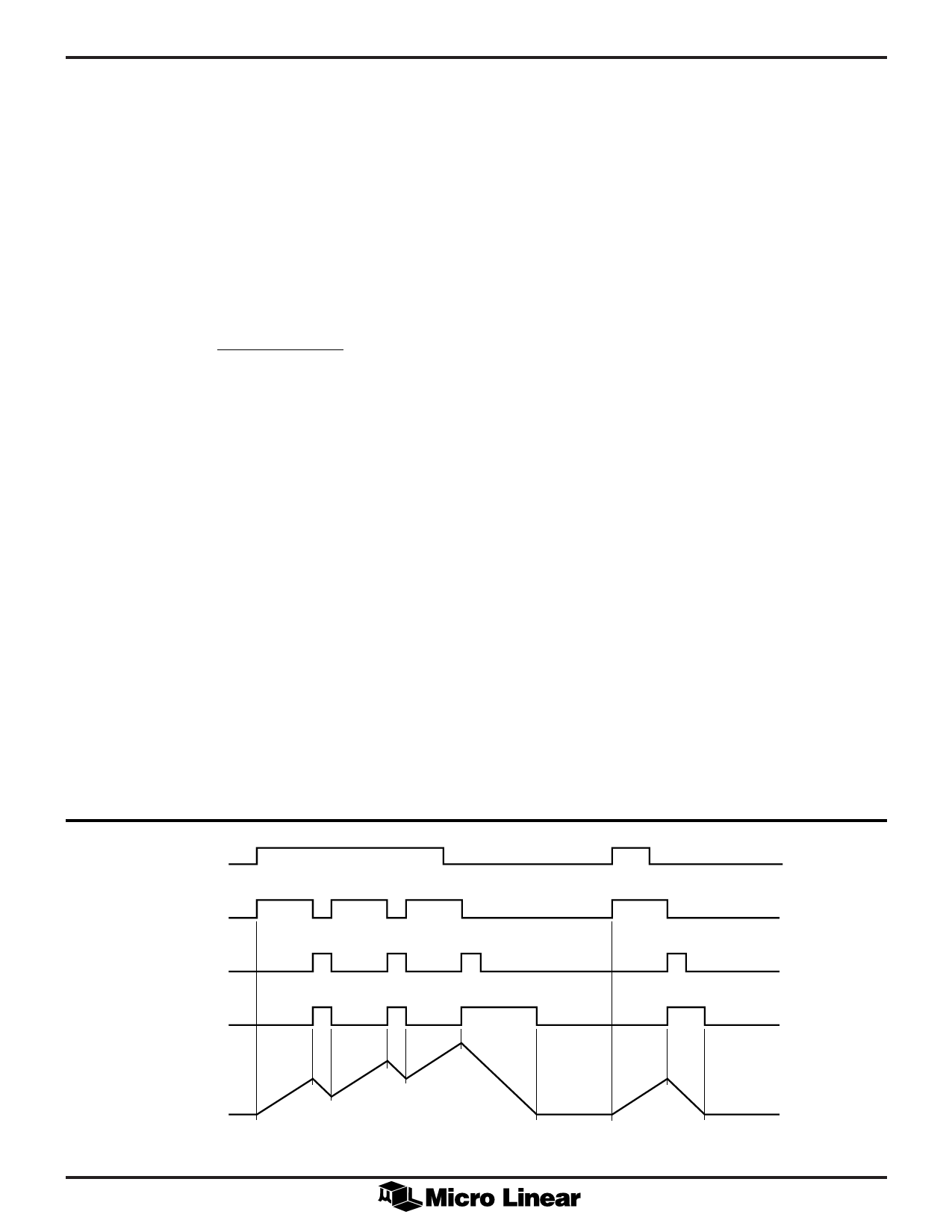
The synchronous rectifier comparator and the two NOR
gates make up the synchronous rectifier control circuit.
The synchronous control does not influence the operation
of the main control loop, and operation with a Schottky
diode in place of the synchronous rectifier is possible, but
at a lower conversion efficiency. The synchronous rectifier
(N DRV) is turned on during the minimum OFF-time or
whenever the ISENSE pin goes below –18mV. N DRV will
remain on until a new ON-time is started or until the
ISENSE pin goes above –18mV. When the ISENSE pin goes
above –18mV, the current in the inductor has gone to zero
VC
TON
TOFF(MIN)
VSR
IL
Figure 2. One Shot and Synchronous Rectifier Timing Diagram
5
Share Link: 