ML4880CS データシートの表示(PDF) - Micro Linear Corporation
部品番号
コンポーネント説明
メーカー
ML4880CS Datasheet PDF : 15 Pages
| |||
ML4880
Having determined the values for the inductor and sense
resistor, we can now specify the inductor peak current
rating. This value is calculated at current limit and at the
maximum input voltage, and is given by:
IL(PK @ MAX) = ISENSE(MAX) + ∆IL(MAX) =
VSENSE(MAX)
RSENSE
+
∆IL(MAX)
=
0.25V
RSENSE
+
∆IL(MAX)
(7)
For reliable operation, the inductor current rating should
exceed the value calculated by 10%-20%.
For future reference, determine the peak inductor current
at the minimum input voltage:
IL(PK @MIN) = ISENSE(MAX) + ∆IL(MIN) =
VSENSE(MAX)
RSENSE
+
∆IL(MIN)
=
0.25V
RSENSE
+
∆IL(MIN)
(8)
Now the sense resistor’s power rating can be determined.
The sense resistor must be able to carry the peak current
in the inductor during the OFF-time:
PRSENSE = IR2MS(OFF) × RSENSE
(9)
where,
IR2MS(OFF)
=
1−
VOUT
VIN(MAX)
(ISENSE(MAX))2
+
(ISENSE(MAX)) (IL(PK @ MAX))
3
+
(IL(PK @MAX))2
One final parameter should be specified: the winding
resistance of the inductor. In general the winding
resistance should be as low as possible, preferably in the
low mΩ range. Since the inductor is in series with the
load at all times, the copper losses can be approximated
by:
PCU = I2OUT × RL
(10)
A good rule of thumb is to allow 2mΩ of winding
resistance per µH of inductance.
BUCK REGULATORS — MOSFET SELECTION
The switching MOSFETs must be logic level types with the
ON resistance specified at VGS = 4.5V. In general, the ON
resistance - gate charge product provides a good figure of
merit by which to compare various MOSFETs, the lower
the figure the better. The internal gate drivers of the
ML4880 can drive over 100nC of total gate charge, but
60nC to 70nC is a more practical limit to ensure good
switching times.
The drain-source breakdown voltage rating is determined
by the input voltage. For input voltages up to 12V, a drain
to source rating of 20V is acceptable. For input voltages
up to 18V, a drain to source rating of 30V is
recommended. For a more reliable design, look for
MOSFETs that are avalanche rated.
In high current applications, the MOSFET’s power
dissipation often becomes a major design factor. The I2R
losses generate the largest portion of heat in the MOSFET
package. Make sure that the MOSFETs are within their
rated junction temperature at the maximum ambient
temperature by calculating the temperature rise using the
thermal resistance specifications.
The worst case power dissipation for the P-MOS switch
occurs at the minimum input voltage and is determined as
follows:
P(P−MOS) = IR2MS(ON) × RDS(ON)
(11)
where
IR2MS(ON)
=
VOUT
VIN(MIN)
(ISENSE(MAX))2
+ (ISENSE(MAX)) (IL(PK @MIN)) + (IL(PK @MIN))2
3
The worst case power dissipation for the N-MOS switch
occurs at the maximum input voltage and is determined
using:
P(N−MOS) = IR2MS(OFF) × RDS(ON)
(12)
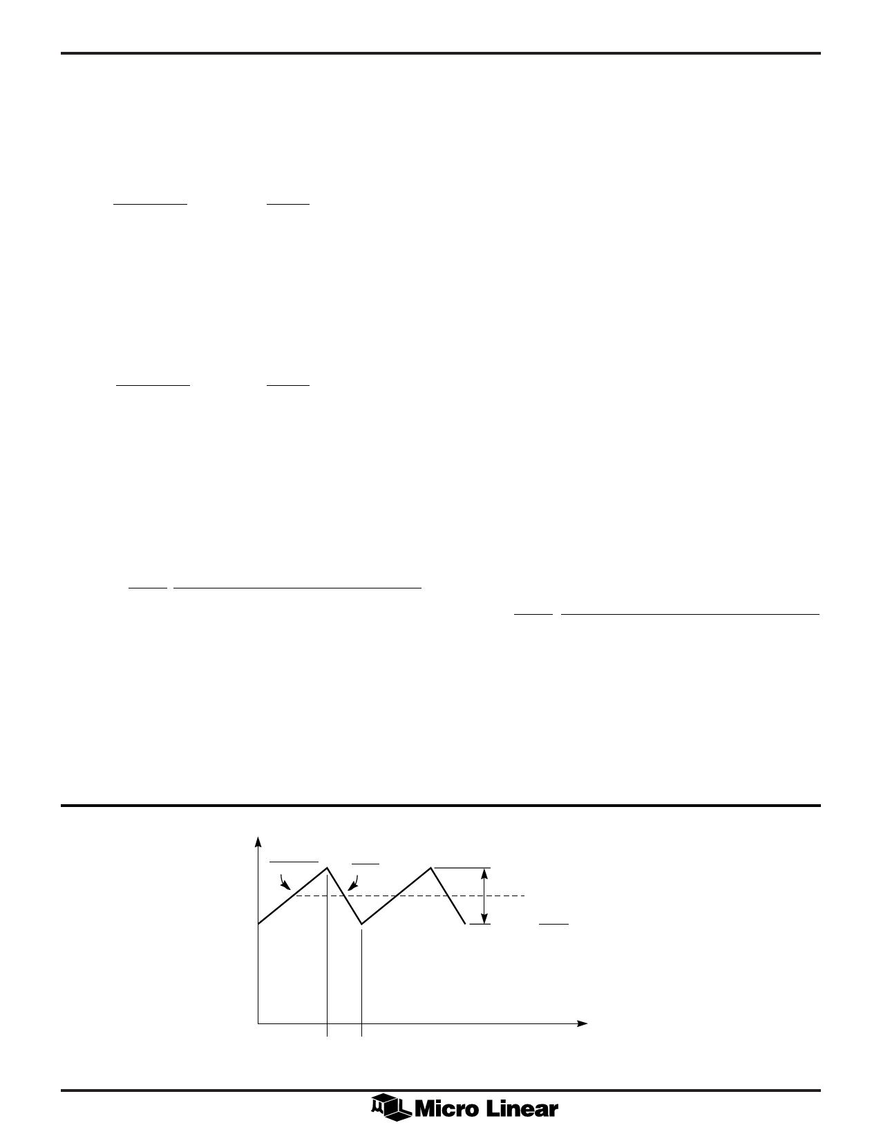
IL
VIN – VOUT
L
VOUT
L
ILPK
∆IL
IOUT = ISENSE + 1/2 ∆IL
ISENSE =
VSENSE
RSENSE
TON
TOFF
t
Figure 6. Buck Regulator Inductor Current
8
Share Link: 