LB1924 データシートの表示(PDF) - SANYO -> Panasonic
部品番号
コンポーネント説明
メーカー
LB1924 Datasheet PDF : 11 Pages
| |||
LB1924
Functional Description
1. Speed control circuit
This IC uses a speed discriminator circuit and a PLL circuit in combination for speed control. The speed control
circuit outputs an error signal once every two FG periods (a charge pump technique). The PLL circuit outputs a phase
error signal once every FG period (also a charge pump technique). As compared with the earlier speed control
technique of using only a speed discriminator, the combined speed discriminator/PLL circuit technique is better able
to suppress speed fluctuations when used with motors with large load variations. The FG servo frequency is
determined by the following equation, which means that the motor speed is determined by the number of FG pulses
and the crystal oscillator frequency.
fFG(servo) = fOSC/8192
fOSC: Crystal oscillator frequency
2. Output drive circuit
This IC adopts a direct PWM drive technique to minimize the power loss in the output. The output transistor is
always saturated when on, and the motor drive power is adjusted by varying the duty with which the output is on.
Since the lower side output transistor is used for output switching, a Schottky diode or similar device must be
connected between OUT and VCC. (This is because a through current will flow at the instant the lower side transistor
turns on unless a diode with a short reverse recovery time is used.) The diode between OUT and ground is included
on chip in this device. If this becomes a problem for large output currents, (e.g. if the output waveform is disturbed
during lower side kickback) attach an external rectifying (or Schottky) diode.
3. Current limiter
The current limiter circuit limits the output to a current determined by the equation I = VRF/Rf, where VRF = 0.5 V
(typical) and Rf is the current detection resistor. The current limiting operation consists of reducing the output on duty
to lower the current.
4. Reference clock
Either of the two following input methods can be used for the speed control clock
• Using a crystal oscillator element
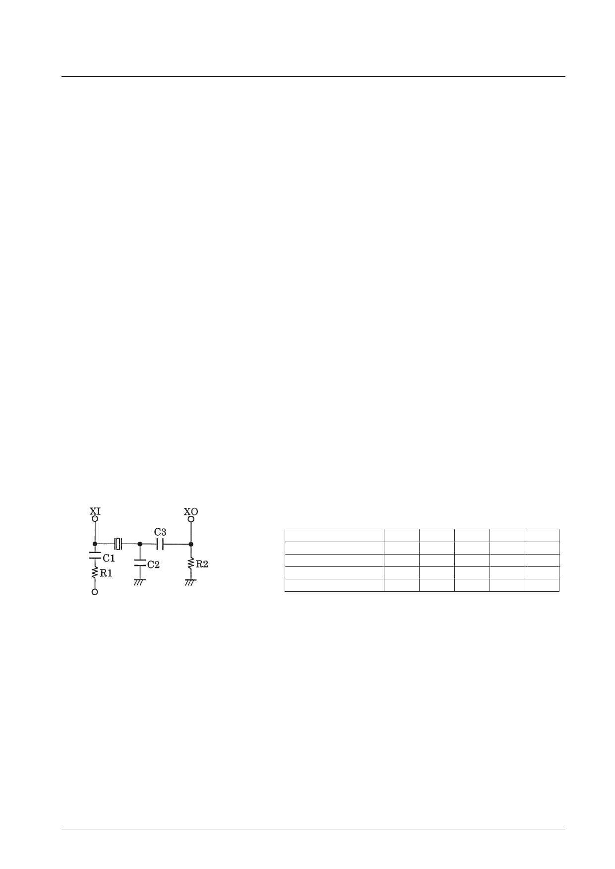
— When using a crystal oscillator element, connect the crystal, capacitors, and resistors as shown in the figure below
to form an oscillator circuit.
Sample External Circuit Constants (Reference values)
VREG
C1, R1: Oscillator stabilization
C3:
Oscillator coupling
C2:
Overtone prevention
R2:
Oscillator operating margin improvement
Oscillator frequency (MHz)
1 to 3
3 to 5
5 to 7
7 to 10
C1 (µF)
0.1
0.1
0.1
0.1
C2 (µF)
47
18
—
—
C3 (µF)
220
100
47
33
R1 (Ω)
220 K
100 K
47 K
10 K
R2 (Ω)
—
—
—
4.7 K
This circuit and these circuit constant values are provided for reference only. Always verify application circuits
with the supplier of the oscillator element to assure that the effects of the characteristics of the oscillator element
itself, the printed circuit board wiring, floating capacitances, and other aspects are accounted for appropriately.
(Notes on printed circuit board lines)
Floating capacitances on the printed circuit board can easily affect crystal oscillator circuits, since these are high-
speed circuits. The printed circuit board lines connecting these components should be kept as short and as narrow
as possible and other measures to reduce floating capacitances should be considered as well.
In this external circuit, the line between the oscillator element and C3 (C2) is particularly subject to floating
capacitance problems and requires special care.
No. 5687-6/11
Share Link: 