NJU6624AFG1 データシートの表示(PDF) - Japan Radio Corporation
部品番号
コンポーネント説明
メーカー
NJU6624AFG1
Japan Radio Corporation

NJU6624AFG1 Datasheet PDF : 35 Pages
| |||
NJU6624A/B
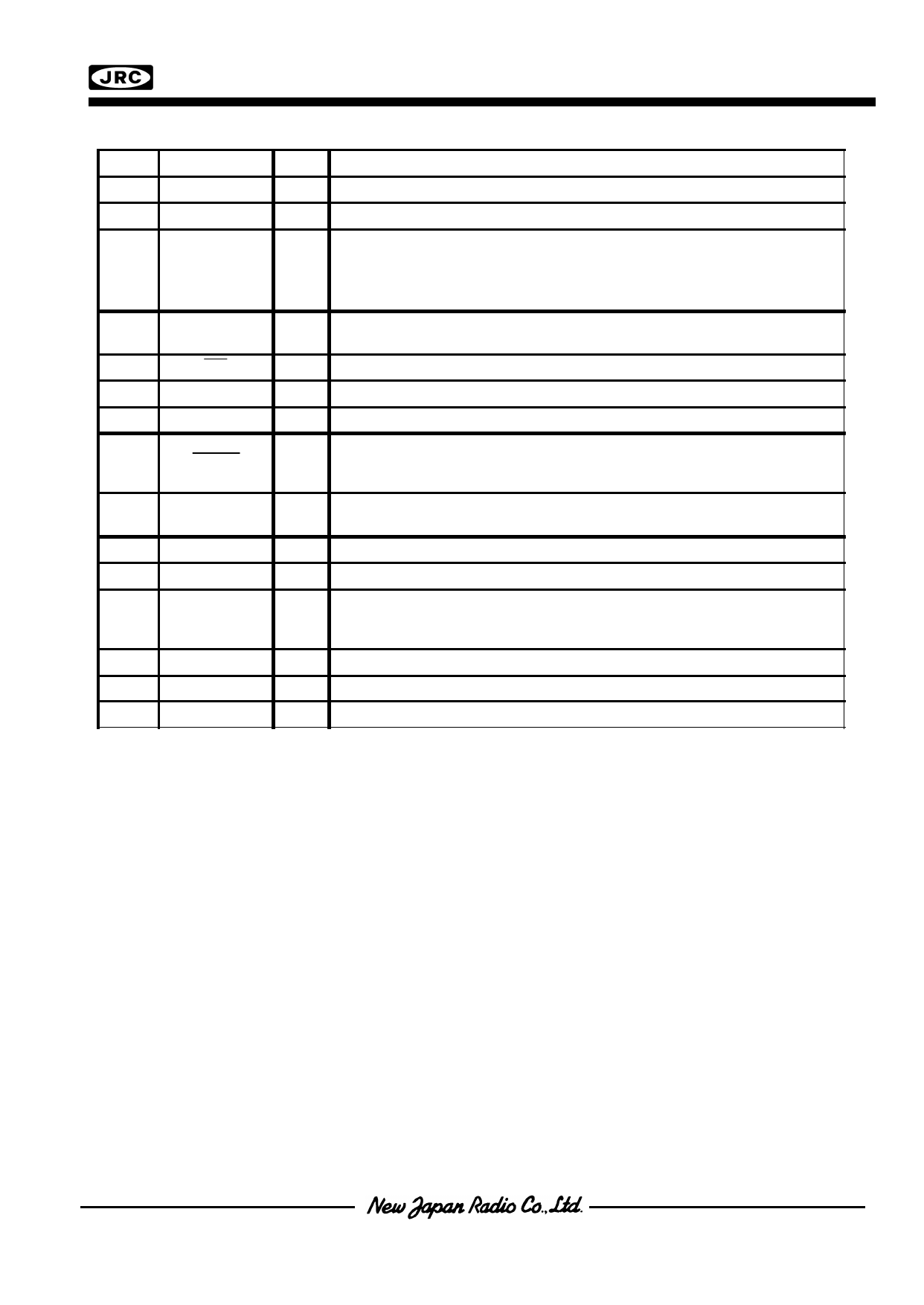
gTERMINAL DESCRIPTION
No.
SYMBOL
2,13 VDD,VSS
1
VLCD1
100
VLCD2
99
V1
98
V2
97
V4
3
OSC1
11
CS
10
SCL
9
DATA
12
RESET
4-7
P0-P3
8
14-17
18-25
26-88
89-95
96
REQ
K0-K3
SEG 1/S0
-
SEG 8/S7
SEG 9-SEG71
COM1-COM7
COMMK
I/O
FUNCTION
- Power Source:VDD=+5V,GND:VSS=0V
I LCD driving voltage input terminal
LCD driving voltage stabilization capacitor terminals.
I
Connect the capacitor between VLCD2 and VSS, V1 and VSS, V2 and
VSS, V4 and VSS.
typ. : 0.1uF
I
System clock input terminal
This terminal should be open for internal clock operation.
I Chip select signal input of serial I/F.
I Sift clock input of serial I/F.
I Serial Data Input of serial I/F.
Reset Terminal.
I When the "L" level is input over than 1.2ms to this terminal,
the system will be reset ( at fOSC 145KHz ).
O
General output port
LED driver drives LED as indicator on athers.
O Key request signal output terminal.
I Key scanning input terminals.
O LCD segment driving signal output / Key scanning output terminals.
O LCD segment driving signal output terminals
O LCD common driving signal output terminals
O Icon common driving signal output terminals
Share Link: