NJU6624AFG1 データシートの表示(PDF) - Japan Radio Corporation
部品番号
コンポーネント説明
メーカー
NJU6624AFG1
Japan Radio Corporation

NJU6624AFG1 Datasheet PDF : 35 Pages
| |||
NJU6624A/B
gFUNCTIONAL DESCRIPTION
(1-1)Register
The NJU6624A/B incorporates two 8-bit registers, an Instruction Register(IR) and a Data Register(DR). The
Register (IR) stores instruction codes such as "Clear Display" and "Cursor Shift" or address data for Display Data
RAM(DD RAM), Character Generator RAM(CG RAM) and Icon Display RAM (MK RAM).
The Register(DR) is a temporary register, the data in the Register(DR) is written into the DD RAM, CG RAM or
MK RAM.
The data in the Register(DR) written by the MPU is transferred automatically to the DD RAM, CG RAM or MK
RAM by internal operation.
These two registers are selected by the selection signal RS as shown below.
(1-2)Address Counter (AC)
The address counter(AC) addresses the DD RAM, CG RAM or MK RAM.
When the address setting instruction is written into the Register(IR), the address information is transferred from
Register(IR) to the Counter(AC). The selection of either the DD RAM, CG RAM or MK RAM is also determined by
this instruction.
After writing (or reading) the display data to (or from) the DD RAM, CG RAM or MK RAM, the Counter(AC) incre-
ments (or decrements) automatically.
(1-3)Display Data RAM (DD RAM)
The display data RAM (DD RAM) consist of 14x 8 bits stores up to 14-character display data represented in 8-bit
code. (2 out of the 14characters are used for scroll RAM.)
The DD RAM address data set in the address counter(AC) is represented in Hexadecimal.
Higher
Lower
A C A C4 A C3 A C 2 A C 1 A C 0
(Example) DD RAM address " 08 "
0
1
0
0
0
HEX.
0
8
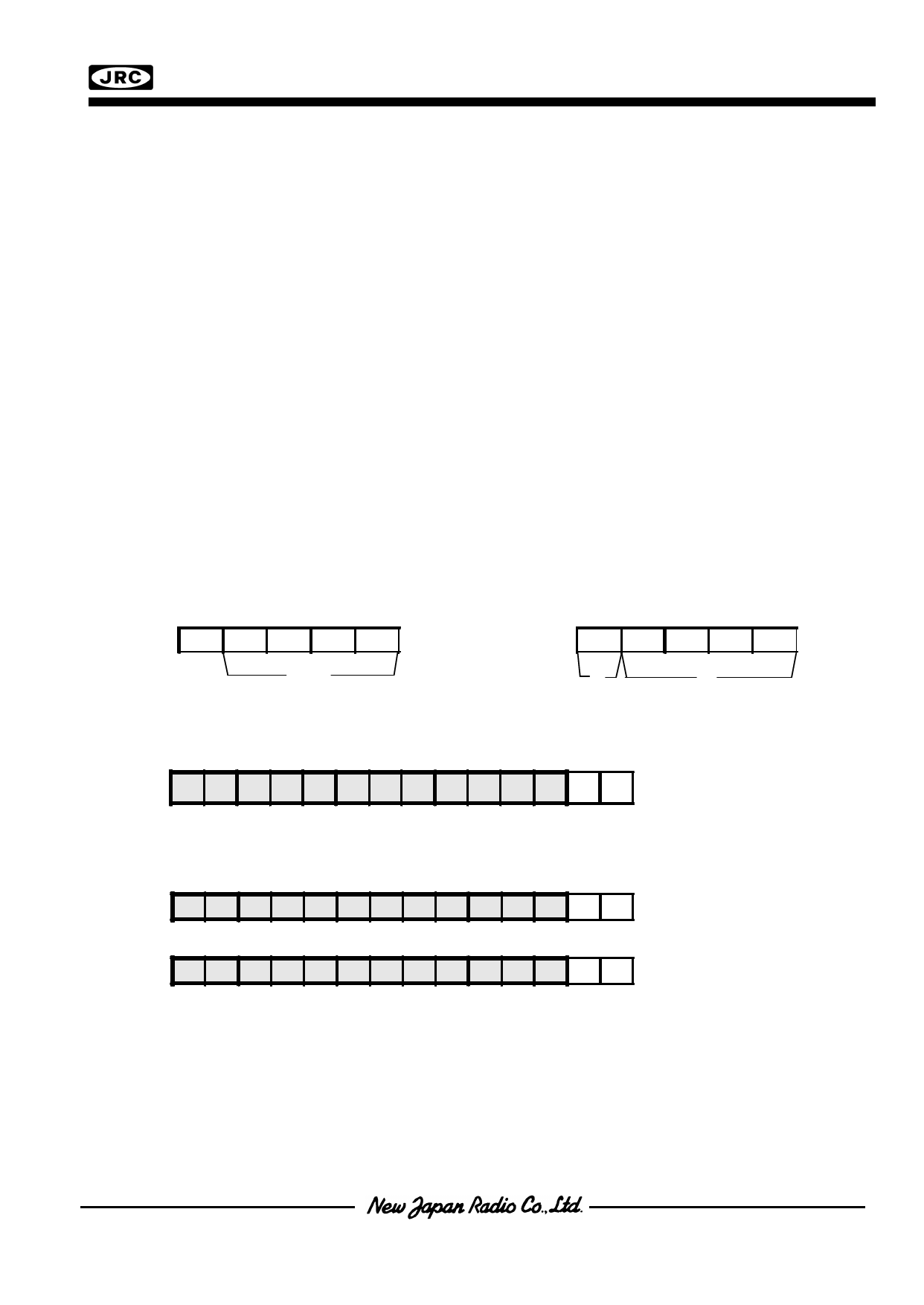
The relation between DD RAM address and display position on the LCD is shown below.
1 2 3 4 5 6 7 8 9 10 11 12 13 14 -Display Position
00 01 02 03 04 05 06 07 08 09 0A 0B 0C 0D -DD RAM Address (Hex.)
| | Scroll RAM
When the display shift is performed,the DD RAM address changes as follows:
( Left Shift Display )
(00)<= 01 02 03 04 05 06 07 08 09 0A 0B 0C 0D 00
( Right Shift Display )
0D 00 01 02 03 04 05 06 07 08 09 0A 0B 0C =>(0E)
(1-4)Character Generator ROM (CG ROM)
The Character Generator ROM (CG ROM) generates 5 x 7 dots character pattern represented in 8-bit character
code.
The storage capacity is up to 224 kinds of 5 x 7 dots character pattern(available address is (20)H through (FF)H).
The correspondence between character code and standard character pattern of NJU6624A/B is shown in Table 2.
User-defined character patterns (Custom Font) are also available by mask option.
Share Link: