SI9993CS データシートの表示(PDF) - Vishay Semiconductors
部品番号
コンポーネント説明
メーカー
SI9993CS Datasheet PDF : 17 Pages
| |||
Si9993CS
Vishay Siliconix
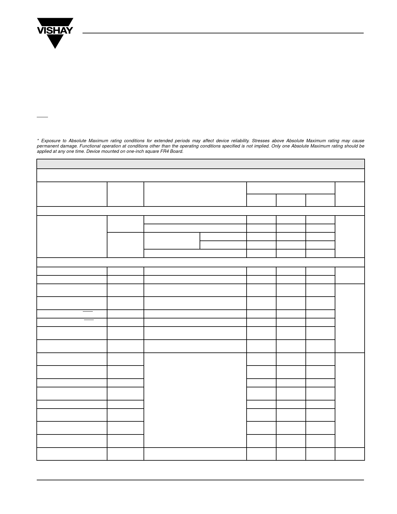
ABSOLUTE MAXIMUM RATINGS (TA = 25°C)*
Voltage Referenced to GND Pin
VDD Supply Range . . . . . . . . . . . . . . . . . . . . . . . . . . . . . . . .-0.3 to 7 V
VCLAMP Supply Range . . . . . . . . . . . . . . . . . . . . . . . . . .> (VCC - 0.3 V
and > (VDD - 0.3 V) to 14 V
VCC, VMOT Supply Range . . . . . . . . . . . . . . . . . . . . . . . . .-0.3 to 14 V
AGND, DGND, PWRGND to GND . . . . . . . . . . . . . . . . . . -0.3 to 0.3 V
SENA, SENB, SENC, CT, VCM+, VCM-Pin . . . . . -1.0 to VCC + 1.0 V
POR, FCOM, STEPCLK, ENCOM, SYSCLK, PWMIN,
PWMOUT, RESETVCM, IPCLK, IPDATA
and IPENABLE pins . . . . . . . . . . . . . . . . . . . . . . . -0.3 to VDD + 0.3 V
All Other Pins . . . . . . . . . . . . . . . . . . . . . . . . . . . . -0.3 to VCC + 0.3 V
Maximum Current (All Input Pins) . . . . . . . . . . . . . . . . . . . . . . ±20 mA
Storage Temperature (Tstg) . . . . . . . . . . . . . . . . . . . . . . . -65 to 150°C
Operating Temperature (TA) . . . . . . . . . . . . . . . . . . . . . . . . . 0 to 70°C
Junction Temperature (TJ). . . . . . . . . . . . . . . . . . . . . . . . . . . . . 150°C
Power Dissipation . . . . . . . . . . . . . . . . . . . . . . . . . . . . . . . . . . . . . 2 W
Thermal Impedance (ΘJA) . . . . . . . . . . . . . . . . . . . . . . . . . . 6.25°C/W
* Exposure to Absolute Maximum rating conditions for extended periods may affect device reliability. Stresses above Absolute Maximum rating may cause
permanent damage. Functional operation at conditions other than the operating conditions specified is not implied. Only one Absolute Maximum rating should be
applied at any one time. Device mounted on one-inch square FR4 Board.
SPECIFICATIONS
Operating Conditions:
VCC = VMOT = 12 V ±10%, VDD = 5 V ±10%, VREF(IN) = VREF(OUT), RSS = RSV = 0.2 Ω ±1%,
RSRADJ = 20 kΩ ±1%, Si9942-Si9430 LITTLE FOOT Driver, FSYSCLK = 5 MHz, TA = 0 to 70°C
Limits
Parameter
Power Supply
Supply Current
Control Logic
Low Input Current
High Input Current
Low Input Voltage
(All Digital Inputs)
High Input Voltage
(All Digital Inputs)
Low Output Voltage (POR)
High Output Voltage (POR)
Low Output Voltage
(FCOM, PWMOUT)
High Output Voltage
(FCOM, PWMOUT)
IPDATA Setup Time to Rising
IPCLK Edge
Rising IPCLK Edge to IPDATA
Hold Time
IPDATA Clock Cycle Time
IPDATA Hold for IPDATA Driver
Turnaround
IPCLK High and Low Time
IPDATA Propagation Delay
WRT IPCLK Falling Edge
IPENABLE Setup Time WRT
IPCLK Rising Edge
IPENABLE Hold Time WRT
IPCLK Rising Edge
WRT IPCLK Falling Edge to
Data Tri-State
Symbol
IDD
ICC + IMOT +
ICLAMP
IIL
IIH
VIL
VIH
VOL
VOH
VOL
VOH
t1
t2
t3
t4
t5
t6
t7
t8
t9
Specific Test Conditions
Normal Operation, Serial Port Idle
D7D6(REG0/5) = 00, All Clocks Disabled
Normal Operation
No Load at VREF(OUT)
With VCM Load
Without VCM Load
D7D6(REG0/5) = 00, All Clocks Disabled
VIN = 0 V
VIN = VDD
IOUT = 4 mA
IOUT = -4 mA
IOUT = 2 mA
IOUT = -2 mA
See Timing Diagram, Figures 1 and 2.
See Timing Diagram, Figures 1 and 2.
Mina
-1
2.0
4.1
4.1
15
15
100
70
45
100
20
Typb
0.2
0.02
40
25
4
10
Maxa
1.2
0.1
65
40
6
1
0.8
0.4
0.4
100
Unit
mA
µA
V
ns
ns
FaxBack 408-970-5600, request 70653
www.siliconix.com
S-60752–Rev. A, 05-Apr-99
3
Share Link: 