PS398CSE データシートの表示(PDF) - Pericom Semiconductor
部品番号
コンポーネント説明
メーカー
PS398CSE Datasheet PDF : 10 Pages
| |||
PS398/PS399
1234567890123456789012345678901212345678901234567890123456789012123456P78r9e01c2i3s4i5o67n89801-2C34h56,7D89i0f1f2.12434-5C67h89,011273V456A789n0a12l3o4g567M890u1l2t1i2p34l5e6x78e9r0s12
Channel
Select
+5V
A2
V+
N01
PS398
A1
N08
A0 GND EN V- COM
1MHz
Capacitance
Analyzer
f =1MHz
-5V
Figure 8. NO/COM Capacitance
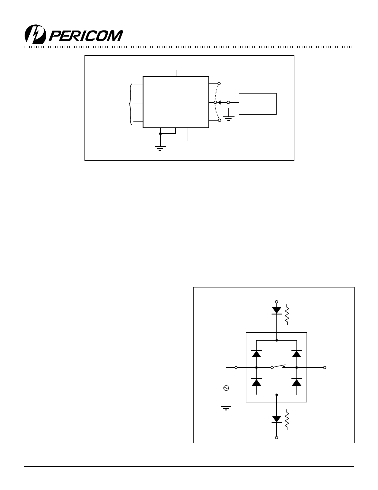
Applications
Overvoltage Protection
Proper power-supply sequencing is recommended for all CMOS
devices. Do not exceed the absolute maximum ratings, because
stresses beyond the listed ratings may cause permanent damage to
the devices. Always sequence V+ on first, followed by V-, and then
logic inputs. If power-supply sequencing is not possible, add two
small signal diodes or two current limiting resistors in series with
the supply pins for overvoltage protection (Figure 9). Adding
diodes reduces the analog signal range, but low switch resistance
and low leakage characteristics are unaffected.
Maximum Sampling Rate
From the sampling theorem, the sampling frequency needed to
properly recover the original signal should be more than twice
its maximum component frequency. In real applications,
sampling at three or four times the maximum signal frequency is
customary.
The maximum sampling rate of a multiplexer is determined by its
transition time (tTRANS), the number of channels being multiplexed,
and the settling time (tSETTLING) of the sampled signal at the out-
put. The maximum sampling rate is:
________1_______
(1)
fS = n (tTRANS + tSETTLING)
Where n = number of channels scanned: 8 for PS398,
4 for PS399. tTRANS is given on the specification table: 150 ns max.
Settling time is the time needed for the output to stabilize within
the desired accuracy band of +1 LSB (least significant bit).
Other factors determining settling time are: signal source imped-
ance, capacitive load at the output. Figure 10 illustrates the steady
state model. To figure out what the settling time due to the multi-
plexer is, we can assume that RS = 0Ω, and CL = 0. In real life, the
effects of RS and CL should be taken into account when perform-
ing these calculations.
Positive Supply
V+
NO
Vg
COM
V-
Figure 9. Overvoltage protection is accomplished using two
external blocking diodes or two current limiting resistors.
9
PS8185C 10/06/99
Share Link: 