KA723D データシートの表示(PDF) - Fairchild Semiconductor
部品番号
コンポーネント説明
メーカー
KA723D Datasheet PDF : 8 Pages
| |||
KA723
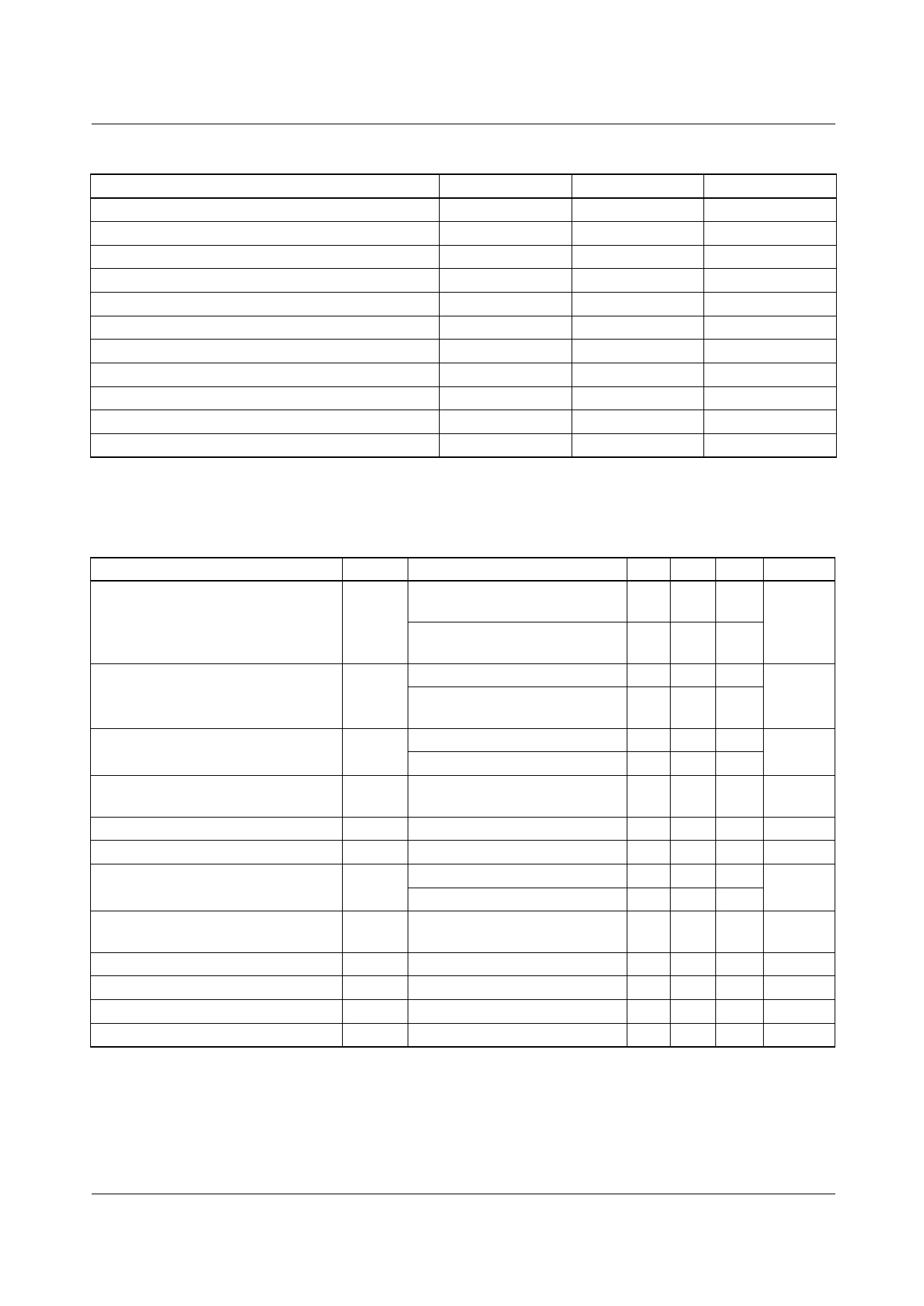
Absolute Maximum Ratings
Parameter
Pulse Voltage from V+ to V- (50ms)
Continuous Voltage from V+ to V-
Input-Output Voltage Differential
Maximum Output Current
Differential Input Voltage
Voltage Between Non-Inverting Input and V-
Current from VZ
Current from VREF
Power Dissipation
Operating Temperature Range
Storage Temperature Range
Symbol
VI(P)
VI
VI - VO
IO
VID
VIE
IZ
IREF
PD
TOPR
TSTG
Value
50
40
40
150
±5
8
25
15
1000
0 ~ +70
-65 ~ + 150
Unit
VPEAK
V
V
mA
V
V
mA
mA
mV
°C
°C
Electrical Characteristics
(Unless otherwise specified, TA = 25°C, VIN =V+= VC = 12V, V-=O,VOUT = 5V, IL =1mA, RSC = 0, CI = 100pF, CREF=0 and
divider impedance as seen by error amplifier ≤10KΩ connected as shown in figure 1)
Parameter
Line Regulation
Load Regulation
Ripple Rejection
Average Temperature Coefficient of
Output Voltage
Short Circuit Current Limit
Reference Voltage
Output Noise Voltage
Long-term Stability
Standby Current Drain
Input Voltage Range
Output Voltage Range
Input-Output Voltage Differential
Symbol
∆VO
∆VO
dB
∆VO/∆T
ISC
VREF
VN
ST
ID
VI
VO
VD
Conditions
Min
VI = 12V to 15V
VI = 12V to 40V
-
TMIN ≤TA≤TMAX
VI = 12V to 15V
-
IO = 1mA to 50mA
-
TMIN ≤T≤TMAX
IO = 1 to 50mA
-
f = 100Hz to 10KHz,CREF =0
-
f = 100Hz to 10KHz,CREF =5µF -
Typ.
0.01
0.1
-
0.03
-
74
86
Max.
0.1
0.5
0.3
0.2
0.6
-
-
TMIN ≤T≤TMAX
- 0.003 0.015
RSC = 10Ω, VO = 0
- 65 -
-
6.80 7.15 7.50
f = 100Hz to 10KHz, CREF = 0 - 20 -
f = 100Hz to 10KHz, CREF=5µF - 2.5 -
-
- 0.1 -
IL = 0, VI = 30V
-
-
-
- 2.0 4.0
9.5 - 40
2.0 - 37
3.0 - 38
Unit
%
%
dB
%/°C
mA
V
µVms
%/
1000HR
mA
V
V
V
Notes:
1.Line and load regulation specifications are given for the condition of constant chip temperature.
2.Temperature drifts must be taken into account separately for hith dissipation conditions.
2
Share Link: 