MAX309CSE(1994) データシートの表示(PDF) - Maxim Integrated
部品番号
コンポーネント説明
メーカー
MAX309CSE
(Rev.:1994)
(Rev.:1994)
Maxim Integrated

MAX309CSE Datasheet PDF : 12 Pages
| |||
Precision, 8-Channel/Dual 4-Channel,
High-Performance, CMOS Analog Multiplexers
______________________________________________________________Pin Description
PIN
MAX308
MAX309
1, 15, 16
—
—
1, 16
2
2
3
3
4–7
—
—
4–7
8
—
—
8, 9
9–12
—
—
10–13
13
14
14
15
NAME
A0, A2, A1
A0, A1
EN
V-
NO1–NO4
NO1A–NO4A
COM
COMA, COMB
NO8–NO5
NO4B–NO1B
V+
GND
FUNCTION
Address Inputs
Address Inputs
Enable Input
Negative Supply Voltage Input
Analog Inputs—bidirectional
Analog Inputs—bidirectional
Analog Output—bidirectional
Analog Outputs—bidirectional
Analog Inputs—bidirectional
Analog Inputs—bidirectional
Positive Supply Voltage Input
Ground
__________Applications Information
Operation with
Supply Voltages Other than 15V
Using supply voltages less than ±15V will reduce the
analog signal range. The MAX308/MAX309 switches
operate with ±4.5V to ±20V bipolar supplies or with a
+4.5V to +30V single supply. Connect V- to GND when
operating with a single supply. Both device types can
also operate with unbalanced supplies, such as +24V
and -5V. The Typical Operating Characteristics graphs
show typical on-resistance with 20V, 15V, 10V, and 5V
supplies. (Switching times increase by a factor of two
or more for operation at 5V.)
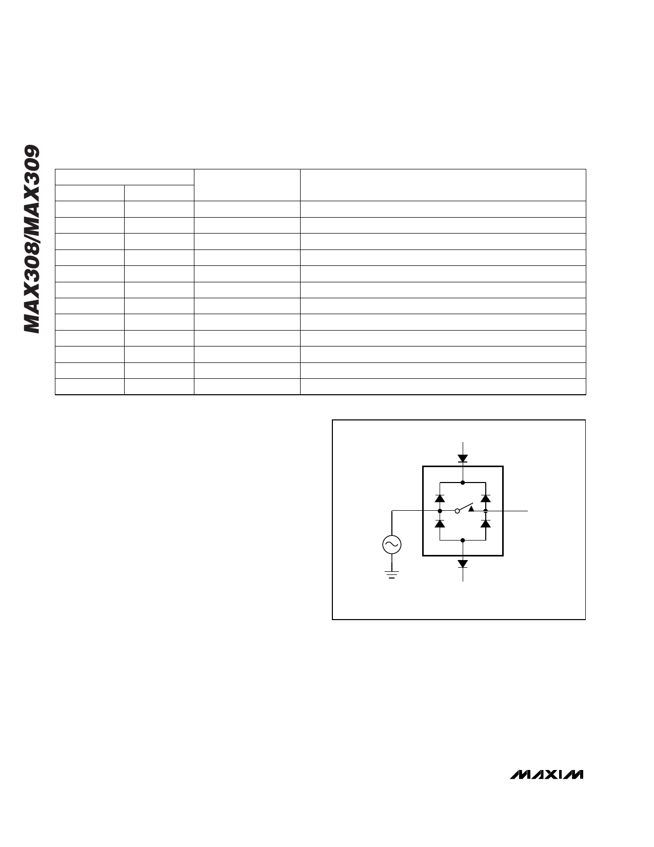
Overvoltage Protection
Proper power-supply sequencing is recommended for
all CMOS devices. Do not exceed the absolute maxi-
mum ratings, because stresses beyond the listed rat-
ings may cause permanent damage to the devices.
Always sequence V+ on first, then V-, followed by the
logic inputs, NO, or COM. If power-supply sequencing
is not possible, add two small signal diodes in series
with supply pins for overvoltage protection (Figure 1).
Adding diodes reduces the analog signal range to 1V
below V+ and 1V above V-, but does not affect the
devices’ low switch resistance and low leakage charac-
teristics. Device operation is unchanged, and the differ-
ence between V+ and V- should not exceed +44V.
V+
NO
COM
Vg
V-
Figure 1. Overvoltage Protection Using External Blocking
Diodes
6 _______________________________________________________________________________________
Share Link: