PS391 データシートの表示(PDF) - Pericom Semiconductor
部品番号
コンポーネント説明
メーカー
PS391 Datasheet PDF : 12 Pages
| |||
PS391/PS392/PS393
11223344556677889900112233445566778899001122334455667788990011221122334455667788990011223344556677889900112233445566778899001122112233445566778899001122334455667788990011223344P5566r7788e99c00i11s22i11o2233n4455,66Q7788u9900a1122d33,44S5566P7788S9900T1122A3344n5566a7788l99o00g1122S1122w3344i55t66c77h8899e0011s22
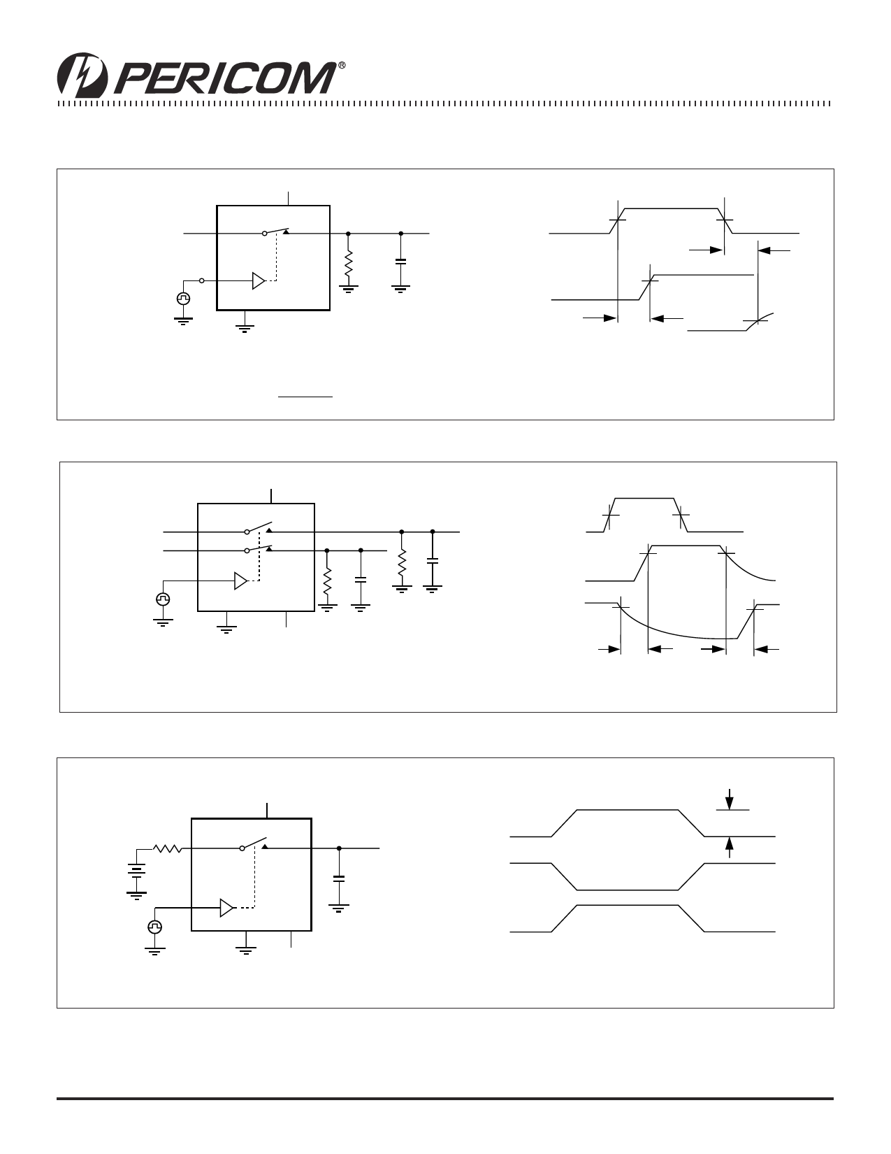
Test Circuits/Timing Diagrams
VCOM = +3V(for ton),
-3V(for toff)
Logic
Input
COM
+12V
V+
NO
or NC
IN
GND
RL
300Ω
VOUT
CL
35pF
Logic +3V
Input
0V
Switch
Output
0V
50%
VOUT
90%
tON
tr <20ns
tf <20ns
tOFF
90%
CL INCLUDES FIXTURE AND STRAY CAPACITANCE
( ) VOUT = VCOM
RL
RL + RON
LOGIC INPUT WAVEFORMS INVERTED FOR
SWITCHES THAT HAVE OPPOSITE LOGIC
Figure 1. Switching Time
+5V
VCOM1= +3V
VCOM3= +3V
Logic
Input
COM
COM
IN
GND
V+
NO
NC
V-
VOUT3
RL2 CL2
VOUT1
RL1 CL1
-5V
RL= 300Ω
CL = 35pF
CL INCLUDES FIXTURE AND STRAY CAPACITANCE
+3V
Logic
Input
0V
Switch
Output 1
(VOUT1) 0V
Switch
Output3
(VOUT3)
0V
50%
90%
tD
Figure 2. Break-Before-Make Interval (PS393 only)
90%
tD
VGEN
RGEN COM
+5V
V+
NO or
NC
Logic
Input
IN
GND V-
-5V
VOUT
CL
1nF
VOUT
IN OFF
OFF
IN
ON
ON
Q = (∆VOUT)(CL)
Figure 3. Charge Injection
∆VOUT
OFF
OFF
10
PS8168E 09/16/02
Share Link: 