AD8005 データシートの表示(PDF) - Analog Devices
部品番号
コンポーネント説明
メーカー
AD8005 Datasheet PDF : 12 Pages
| |||
APPLICATIONS
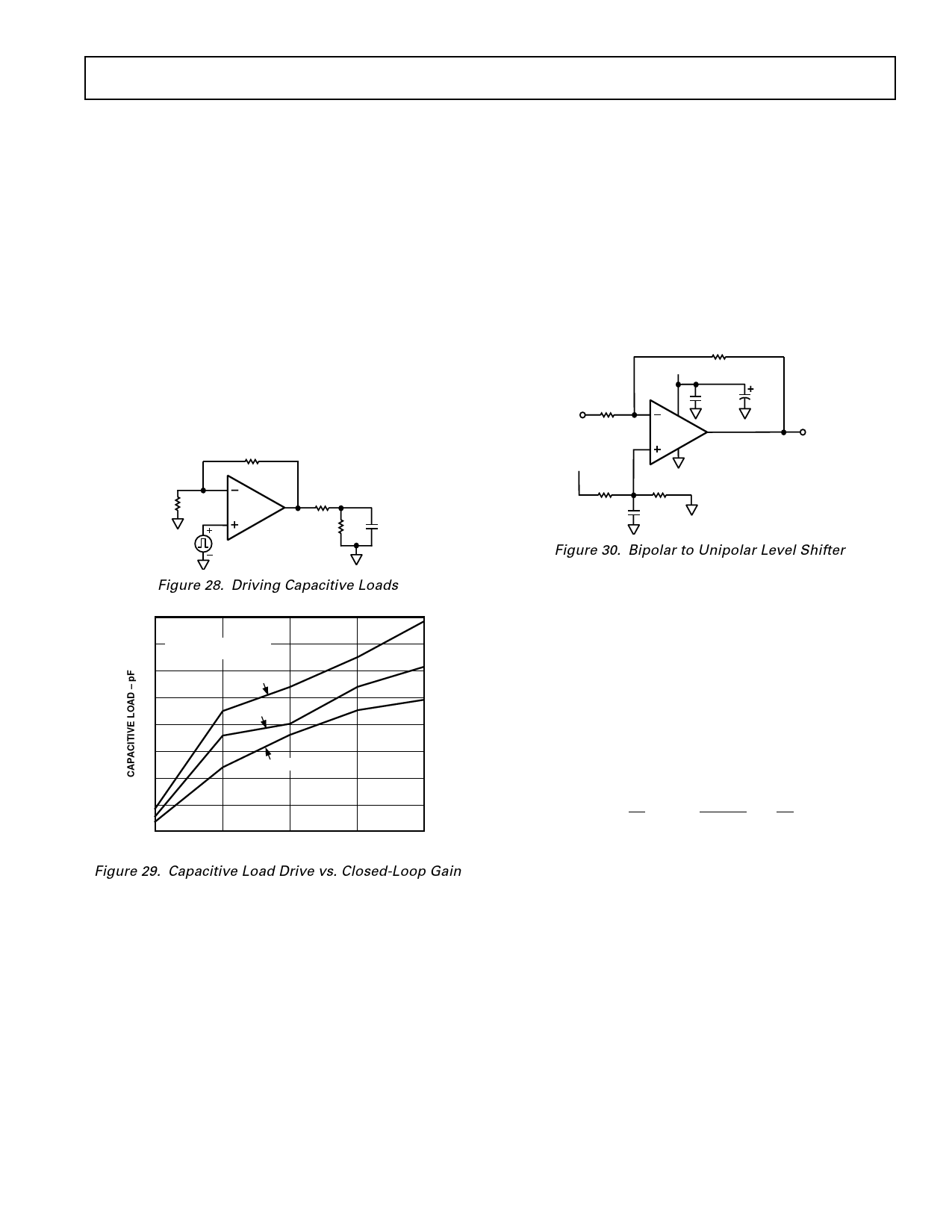
Driving Capacitive Loads
Capacitive loads interact with an op amp’s output impedance
to create an extra delay in the feedback path. This reduces
circuit stability, and can cause unwanted ringing and oscilla-
tion. A given value of capacitance causes much less ringing
when the amplifier is used with a higher noise gain.
The capacitive load drive of the AD8005 can be increased by
adding a low valued resistor in series with the capacitive load.
Introducing a series resistor tends to isolate the capacitive load
from the feedback loop thereby diminishing its influence. Fig-
ure 29 shows the effects of a series resistor on capacitive drive
for varying voltage gains. As the closed-loop gain is increased,
the larger phase margin allows for larger capacitive loads with
less overshoot. Adding a series resistor at lower closed-loop
gains accomplishes the same effect. For large capacitive loads,
the frequency response of the amplifier will be dominated by
the roll-off of the series resistor and capacitive load.
RF
RG
RS
AD8005
RL
1k⍀
CL
Figure 28. Driving Capacitive Loads
80
VS = ؎5V
70 2V OUTPUT STEP
WITH 30% OVERSHOOT
60
RS = 10⍀
50
RS = 5⍀
40
30
RS = 0⍀
20
10
0
1
2
3
4
5
CLOSED-LOOP GAIN – V/V
Figure 29. Capacitive Load Drive vs. Closed-Loop Gain
AD8005
Single-Supply Level Shifter
In addition to providing buffering, many systems require that an
op amp provide level shifting. A common example is the level
shifting that is required to move a bipolar signal into the unipo-
lar range of many modern analog-to-digital converters (ADCs). In
general, single supply ADCs have input ranges that are refer-
enced neither to ground nor supply. Instead the reference level
is some point in between, usually halfway between ground and
supply (+2.5 V for a single supply 5 V ADC). Because high-
speed ADCs typically have input voltage ranges of 1 V to 2 V,
the op amp driving it must be single supply but not necessarily
rail-to-rail.
R2
1.5k⍀
+5V
R1
1.5k⍀
VIN
VREF
+5V
R3
30.1k⍀
0.01F 10F
AD8005
R4
10k⍀
VOUT
0.1F
Figure 30. Bipolar to Unipolar Level Shifter
Figure 30 shows a level shifter circuit that can move a bipolar
signal into a unipolar range. A positive reference voltage, derived
from the +5 V supply, sets a bias level of +1.25 V at the nonin-
verting terminal of the op amp. In ac applications, the accuracy of
this voltage level is not important. Noise is however a serious
consideration. A 0.1 µF capacitor provides useful decoupling of
this noise.
The bias level on the noninverting terminal sets the input common-
mode voltage to +1.25 V. Because the output will always be
positive, the op amp may therefore be powered with a single
+5 V power supply.
The overall gain function is given by the equation:
V OUT
=
–
R2
R1
V IN
+
R4
R3 + R4
1+
R2
R1
V
REF
In the above example, the equation simplifies to
VOUT = –V IN + 2.5V
REV. A
–9–
Share Link: 