NCV431A(2012) データシートの表示(PDF) - ON Semiconductor
部品番号
コンポーネント説明
メーカー
NCV431A Datasheet PDF : 18 Pages
| |||
TL431, A, B Series, NCV431A, B
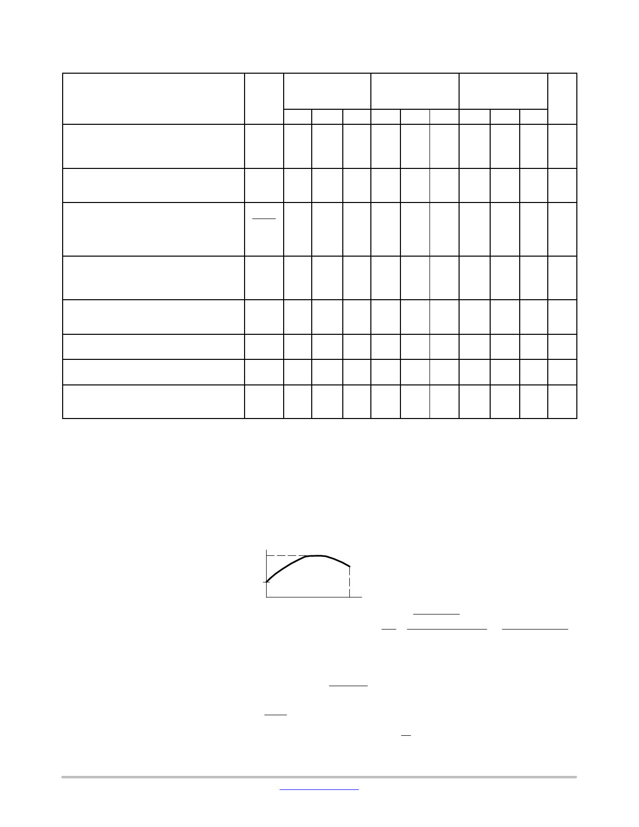
ELECTRICAL CHARACTERISTICS (TA = 25°C, unless otherwise noted.)
TL431AI / NCV431AI
TL431AC
TL431BC / TL431BI /
TL431BV /
NCV431BV
Characteristic
Symbol Min Typ Max Min Typ Max Min Typ Max Unit
Reference Input Voltage (Figure 1)
VKA = Vref, IK = 10 mA
TA = 25°C
TA = Tlow to Thigh
Reference Input Voltage Deviation Over
Temperature Range (Figure 1, Notes 4, 5)
VKA= Vref, IK = 10 mA
Ratio of Change in Reference Input Voltage to
Change in Cathode to Anode Voltage
IK = 10 mA (Figure 2),
DVKA = 10 V to Vref
DVKA = 36 V to 10 V
Reference Input Current (Figure 2)
IK = 10 mA, R1 = 10 k, R2 = ∞
TA = 25°C
TA = Tlow to Thigh (Note 4)
Reference Input Current Deviation Over
Temperature Range (Figure 2, Note 4)
IK = 10 mA, R1 = 10 k, R2 = ∞
Minimum Cathode Current For Regulation
VKA = Vref (Figure 1)
Off−State Cathode Current (Figure 3)
VKA = 36 V, Vref = 0 V
Dynamic Impedance (Figure 1, Note 6)
VKA = Vref, DIK = 1.0 mA to 100 mA
f ≤ 1.0 kHz
Vref
DVref
V
2.47 2.495 2.52 2.47 2.495 2.52 2.485 2.495 2.505
2.44 − 2.55 2.453 − 2.537 2.475 2.495 2.515
− 7.0 30
− 3.0 17
−
3.0 17 mV
DVref
mV/V
DVKA
− −1.4 −2.7 − −1.4 −2.7 − −1.4 −2.7
− −1.0 −2.0 − −1.0 −2.0 − −1.0 −2.0
Iref
mA
−
1.8 4.0
−
1.8 4.0
−
1.1 2.0
−
− 6.5 −
−
5.2
−
− 4.0
DIref
− 0.8 2.5 − 0.4 1.2
−
0.8 2.5 mA
Imin
Ioff
|ZKA|
−
0.5 1.0
−
0.5 1.0
−
0.5 1.0 mA
−
20 1000 −
20 1000 − 0.23 500 nA
− 0.22 0.5
− 0.22 0.5
− 0.14 0.3 W
4. Tlow = −40°C for TL431AIP TL431AILP, TL431IP, TL431ILP, TL431BID, TL431BIP, TL431BILP, TL431BV, TL431AIDM, TL431IDM,
TL431BIDM, NCV431AIDMR2G, NCV431AIDR2G, NCV431BVDR2G
= 0°C for TL431ACP, TL431ACLP, TL431CP, TL431CLP, TL431CD, TL431ACD, TL431BCD, TL431BCP, TL431BCLP, TL431CDM,
TL431ACDM, TL431BCDM
Thigh = +85°C for TL431AIP, TL431AILP, TL431IP, TL431ILP, TL431BID, TL431BIP, TL431BILP, TL431IDM, TL431AIDM, TL431BIDM
= +70°C for TL431ACP, TL431ACLP, TL431CP, TL431ACD, TL431BCD, TL431BCP, TL431BCLP, TL431CDM, TL431ACDM,
TL431BCDM
= +125°C TL431BV, NCV431AIDMR2G, NCV431AIDR2G, NCV431BVDMR2G, NCV431BVDR2G
5. The deviation parameter DVref is defined as the difference between the maximum and minimum values obtained over the full operating
ambient temperature range that applies.
Vref max
Vref min
DVref = Vref max
-Vref min
DTA = T2 - T1
T1 Ambient Temperature T2
The average temperature coefficient of the reference input voltage, aVref is defined as:
ǒ Ǔ Vref
ppm
_C
+
D Vref
Vref @ 25_C
D TA
X 106
+
D Vref x 106
D TA (Vref @ 25_C)
aVref can be positive or negative depending on whether Vref Min or Vref Max occurs at the lower ambient temperature. (Refer to Figure 6.)
Example : DVref + 8.0 mV and slope is positive,
Vref @ 25_C + 2.495 V, DTA + 70_C
0.008 x 10⁶
a Vref + 70 (2.495) + 45.8 ppmń_C
6.
The
dynamic
impedance
ZKA
is
defined
as
|ZKA|
+
D VKA
D IK
When
the
device
is
programmed
with
two
external
resistors,
R1
and
R2,
(refer
ǒ Ǔ to Figure 2) the total dynamic impedance of the circuit is defined as: |ZKAȀ| [ |ZKA|
1
)
R1
R2
7. NCV431AIDMR2G, NCV431AIDR2G, NCV431BVDMR2G, NCV431BVDR2G Tlow = −40°C, Thigh = +125°C. Guaranteed by design.
NCV prefix is for automotive and other applications requiring unique site and control change requirements.
http://onsemi.com
4
Share Link: 