TIP33CG データシートの表示(PDF) - ON Semiconductor
部品番号
コンポーネント説明
メーカー
TIP33CG Datasheet PDF : 6 Pages
| |||
500
200
100
50
20
10
5.0
0.1
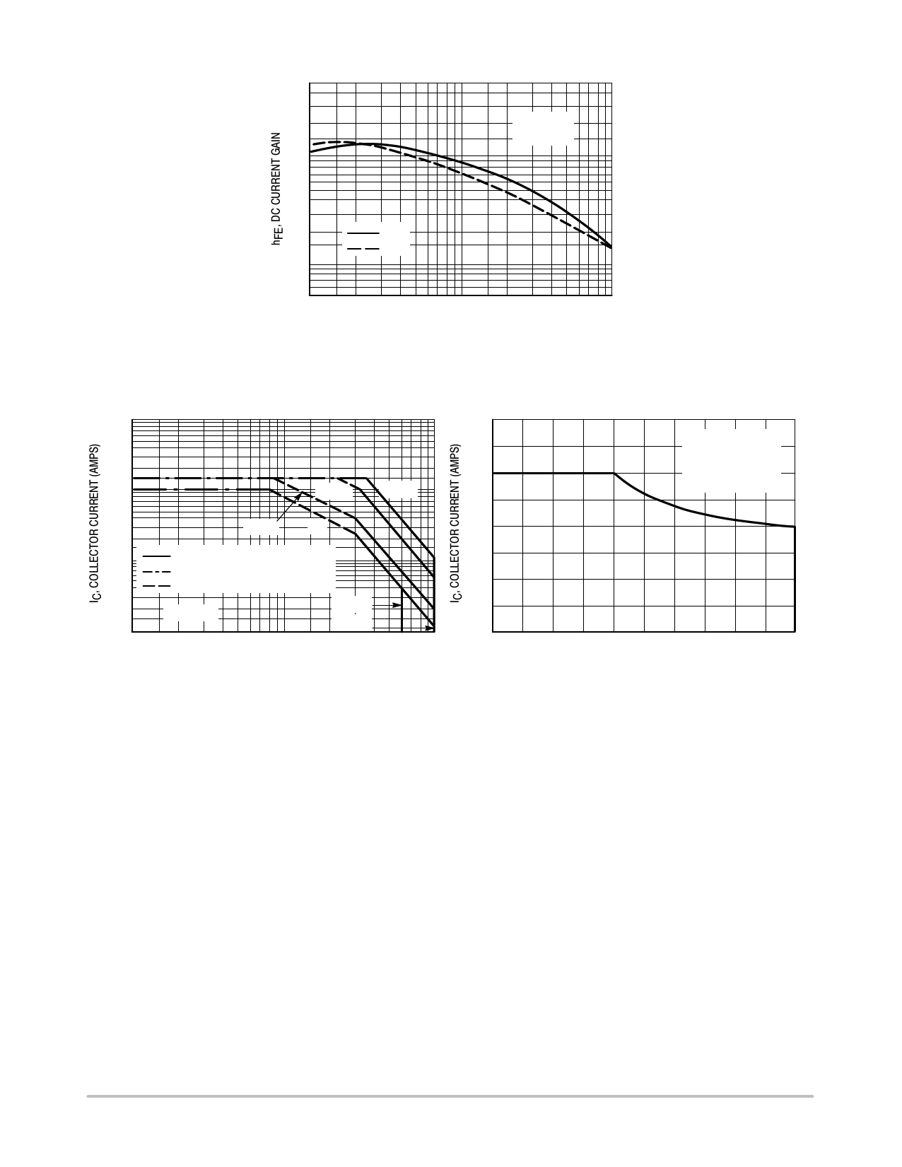
TIP33A, TIP33C
VCE = 4.0 V
TJ = 25°C
NPN
PNP
1.0
10
IC, COLLECTOR CURRENT (A)
Figure 1. DC Current Gain
15
10
5.0
3.0
2.0
1.0
0.5
0.2
0.1
1.0
1.0 ms
300 ms
10 ms
dc
SECONDARY BREAKDOWN LIMIT
BONDING WIRE LIMIT
THERMAL LIMIT
TC = 25°C
TIP33A
TIP33C
2.0 3.0 5.0 7.0 10
20 30 50
VCE, COLLECTOR-EMITTER VOLTAGE (VOLTS)
70 100
Figure 2. Maximum Rated Forward Bias
Safe Operating Area
20
L = 200 mH
IC/IB ≥ 5.0
15
VBE(off) = 0 to 5.0 V
TC = 100°C
10
5.0
0
0
20
40
60
80
100
VCE, COLLECTOR-EMITTER VOLTAGE (VOLTS)
Figure 3. Maximum Rated Forward Bias
Safe Operating Area
FORWARD BIAS
The Forward Bias Safe Operating Area represents the
voltage and current conditions these devices can withstand
during forward bias. The data is based on TC = 25_C; TJ(pk)
is variable depending on power level. Second breakdown
pulse limits are valid for duty cycles to 10%, and must be
derated thermally for TC > 25_C.
REVERSE BIAS
The Reverse Bias Safe Operating Area represents the
voltage and current conditions these devices can withstand
during reverse biased turn−off. This rating is verified under
clamped conditions so the device is never subjected to an
avalanche mode.
http://onsemi.com
4
Share Link: 