LA7790M データシートの表示(PDF) - SANYO -> Panasonic
部品番号
コンポーネント説明
メーカー
LA7790M Datasheet PDF : 14 Pages
| |||
LA7790M
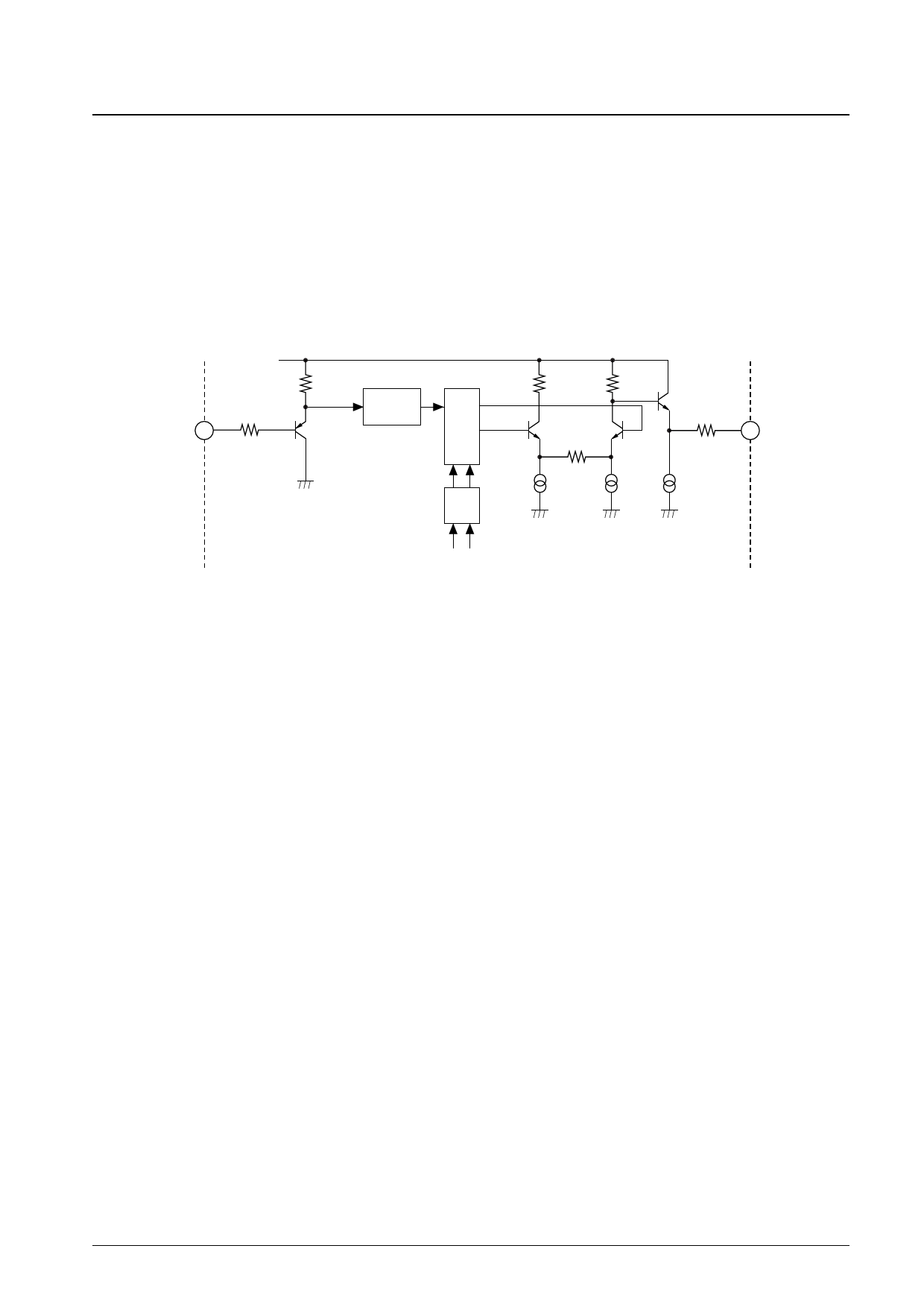
2. Attenuator
The attenuator input signal comes from the modulator output via a high pass filter (fC = 2 MHz). The modulator
output is pin 19. Pin 19 is connected to the emitter of an NPN emitter follower through a 100 Ω resistor. The emitter
sink current is about 1 mA, but can be increased by the addition of an external resistor between pin 19 and ground.
The minimum value for the external resistor is 1.5 kΩ.
The output level of pin 19 can be adjusted using pin 21. Pin 21 is connected to the base of a PNP emitter follower
through a 300 Ω resistor. When pin 21 = 0 V, the base current is about 10 µA.
Equivalent circuit of attenuator block
VCC
Gain
300
control 21
0 to 10 µA
Control
Circuit
ATT
1k
1k
1k
100
19
MOD
output
HPF
1 mA
From Modulator
1 mA 1 mA
Unit (resistance : Ω)
3. RF Amplifier
The RF amplifier input signal comes from the attenuator output after the harmonics are removed by the LPF. The RF
amplifier is composed of a two-stage amplifier and includes mute and power save functions.
The gain of the RF amplifier can be adjusted using the external input resistor connected to pin 22 and the external
load resistor connected to pin 1. The input of pin 22 must be AC coupled. The output of pin 1 must be connected to
VCC via a choke coil. Pin 23 (mute control) and pin 20 (power save control) are both high impedance inputs (base
current less than 10 µA). For normal operation, the voltage at pins 20 and 23 must be less than 1 V. For Mute and
Power Save operation, the voltage at pins 20 are 23 must be between VCC–1 and VCC.
No. 5689-10/14
Share Link: 