SN74LS298N データシートの表示(PDF) - Motorola => Freescale
部品番号
コンポーネント説明
メーカー
SN74LS298N Datasheet PDF : 6 Pages
| |||
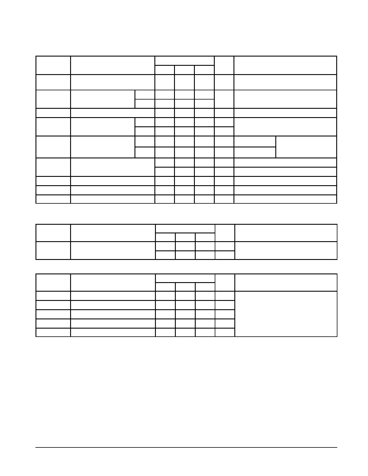
SN54 / 74LS298
DC CHARACTERISTICS OVER OPERATING TEMPERATURE RANGE (unless otherwise specified)
Limits
Symbol
Parameter
Min Typ Max Unit
Test Conditions
VIH
Input HIGH Voltage
2.0
V
Guaranteed Input HIGH Voltage for
All Inputs
54
VIL
Input LOW Voltage
74
0.7
Guaranteed Input LOW Voltage for
0.8
V
All Inputs
VIK
VOH
Input Clamp Diode Voltage
54
Output HIGH Voltage
74
– 0.65 – 1.5
2.5
3.5
2.7
3.5
V
VCC = MIN, IIN = – 18 mA
V
VCC = MIN, IOH = MAX, VIN = VIH
V
or VIL per Truth Table
VOL
Output LOW Voltage
54, 74
74
0.25 0.4
0.35 0.5
V
IOL = 4.0 mA
VCC = VCC MIN,
VIN = VIL or VIH
V
IOL = 8.0 mA
per Truth Table
IIH
Input HIGH Current
20
µA VCC = MAX, VIN = 2.7 V
0.1
mA VCC = MAX, VIN = 7.0 V
IIL
Input LOW Current
– 0.4 mA VCC = MAX, VIN = 0.4 V
IOS
Short Circuit Current (Note 1)
– 20
– 100 mA VCC = MAX
ICC
Power Supply Current
21
Note 1: Not more than one output should be shorted at a time, nor for more than 1 second.
mA VCC = MAX
AC CHARACTERISTICS (TA = 25°C, VCC = 5.0 V)
Limits
Symbol
Parameter
Min Typ Max Unit
tPLH
tPHL
Propagation Delay,
Clock to Output
18
27
ns
21
32
ns
Test Conditions
VCC = 5.0 V,
CL = 15 pF
AC SET-UP REQUIREMENTS (TA = 25°C, VCC = 5.0 V)
Limits
Symbol
Parameter
Min Typ Max Unit
tW
Clock Pulse Width
20
ns
ts
Data Setup Time
15
ns
ts
Select Setup Time
25
ns
th
Data Hold Time
5.0
ns
th
Select Hold Time
0
Test Conditions
VCC = 5.0 V
DEFINITIONS OF TERMS
SETUP TIME (ts) — is defined as the minimum time required
for the correct logic level to be present at the logic input prior to
the clock transition from LOW to HIGH in order to be recog-
nized and transferred to the outputs.
HOLD TIME (th) — is defined as the minimum time following
the clock transition from LOW to HIGH that the logic level must
be maintained at the input in order to ensure continued recog-
nition. A negative HOLD TIME indicates that the correct logic
level may be released prior to the clock transition from LOW to
HIGH and still be recognized.
FAST AND LS TTL DATA
5-475
Share Link: 