MC1489 データシートの表示(PDF) - Motorola => Freescale
部品番号
コンポーネント説明
メーカー
MC1489 Datasheet PDF : 6 Pages
| |||
MC1489, A
MAXIMUM RATINGS (TA = + 25°C, unless otherwise noted)
Rating
Symbol
Power Supply Voltage
Input Voltage Range
Output Load Current
Power Dissipation (Package Limitation, SO–14
and Plastic Dual In–Line Package)
Derate above TA = + 25°C
Operating Ambient Temperature Range
Storage Temperature Range
VCC
VIR
IL
PD
1/θJA
TA
Tstg
Value
10
± 30
20
1000
6.7
0 to + 75
– 65 to + 175
Unit
Vdc
Vdc
mA
mW
mW/°C
°C
°C
ELECTRICAL CHARACTERISTICS (Response control pin is open.) (VCC = + 5.0 Vdc ± 10%, TA = 0 to + 75°C, unless otherwise noted)
Characteristics
Symbol
Min
Typ
Max
Unit
Positive Input Current
Negative Input Current
p Input Turn–On Threshold Voltage
(TA = + 25°C, VOL 0.45 V)
(VIH = + 25 Vdc)
(VIH = + 3.0 Vdc)
(VIH = – 25 Vdc)
(VIH = – 3.0 Vdc)
MC1489
MC1489A
IIH
3.6
–
8.3
mA
0.43
–
–
IIL
– 3.6
–
– 8.3
mA
– 0.43
–
–
VIH
Vdc
1.0
–
1.5
1.75
1.95
2.25
q Input Turn–Off Threshold Voltage
(TA = + 25°C, VOH 2.5 V, IL = – 0.5 mA)
MC1489
MC1489A
VIL
Vdc
0.75
–
1.25
0.75
0.8
1.25
Output Voltage High
(VIH = 0.75 V, IL = – 0.5 mA)
(Input Open Circuit, IL = – 0.5 mA)
Output Voltage Low
Output Short–Circuit Current
(VIL = 3.0 V, IL = 10 mA)
Power Supply Current (All Gates “on,” Iout = 0 mA, VIH = + 5.0 Vdc)
VOH
VOL
IOS
ICC
2.5
4.0
5.0
Vdc
2.5
4.0
5.0
–
0.2
0.45
Vdc
–
– 3.0 – 4.0
mA
–
16
26
mA
Power Consumption
(VIH = + 5.0 Vdc)
PC
SWITCHING CHARACTERISTICS (VCC = 5.0 Vdc ± 1%, TA = + 25°C, See Figure 1.)
Propagation Delay Time
(RL = 3.9 kΩ)
tPLH
Rise Time
(RL = 3.9 kΩ)
tTLH
Propagation Delay Time
(RL = 390 kΩ)
tPHL
Fall Time
(RL = 390 kΩ)
tTHL
–
80
130
mW
–
25
85
ns
–
120
175
ns
–
25
50
ns
–
10
20
ns
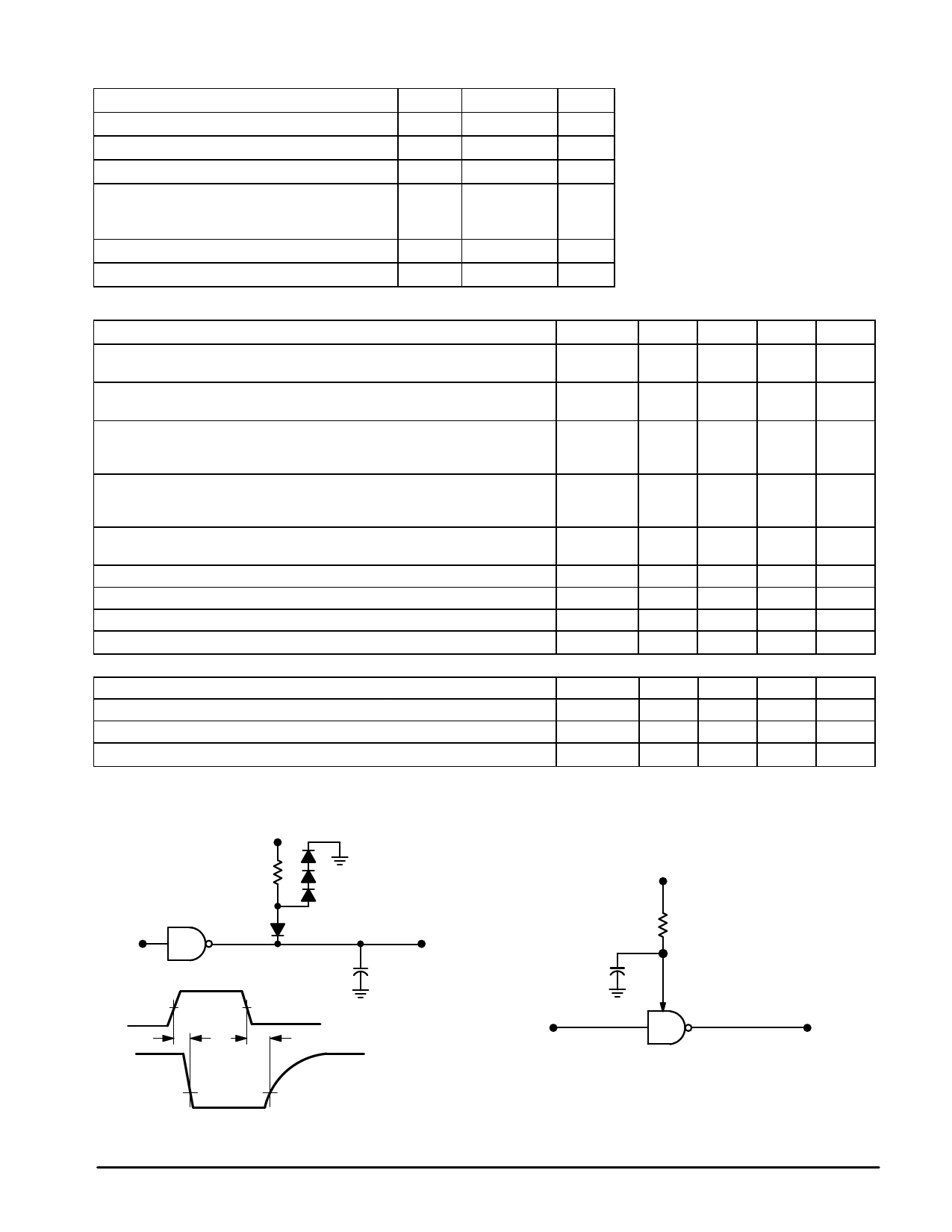
Figure 1. Switching Response
5.0 Vdc
TEST CIRCUITS
RL
All diodes
1N3064
or equivalent
Ein
Eo
CL
3.0 V
50%
50%
Ein
EO
tTLH and tTHL
tPLH
measured
10% – 90%
Vin
tTHL 1.5 V
tTLH
1.5 V
CL = 15 pF = total parasitic capacitance which includes
probe and wiring capacitances
Figure 2. Response Control Node
VR
R
C
1/4
Response Node
MC1489A
VO
C, capacitor is for noise filtering.
R, resistor is for threshold shifting.
2
MOTOROLA ANALOG IC DEVICE DATA
Share Link: 