TLIU04C1 データシートの表示(PDF) - Agere -> LSI Corporation
部品番号
コンポーネント説明
メーカー
TLIU04C1 Datasheet PDF : 100 Pages
| |||
TLIU04C1 Quad T1/E1 Line Interface
Advance Data Sheet, Rev. 2
April 1999
Microprocessor Mode (continued)
Pin Information (continued)
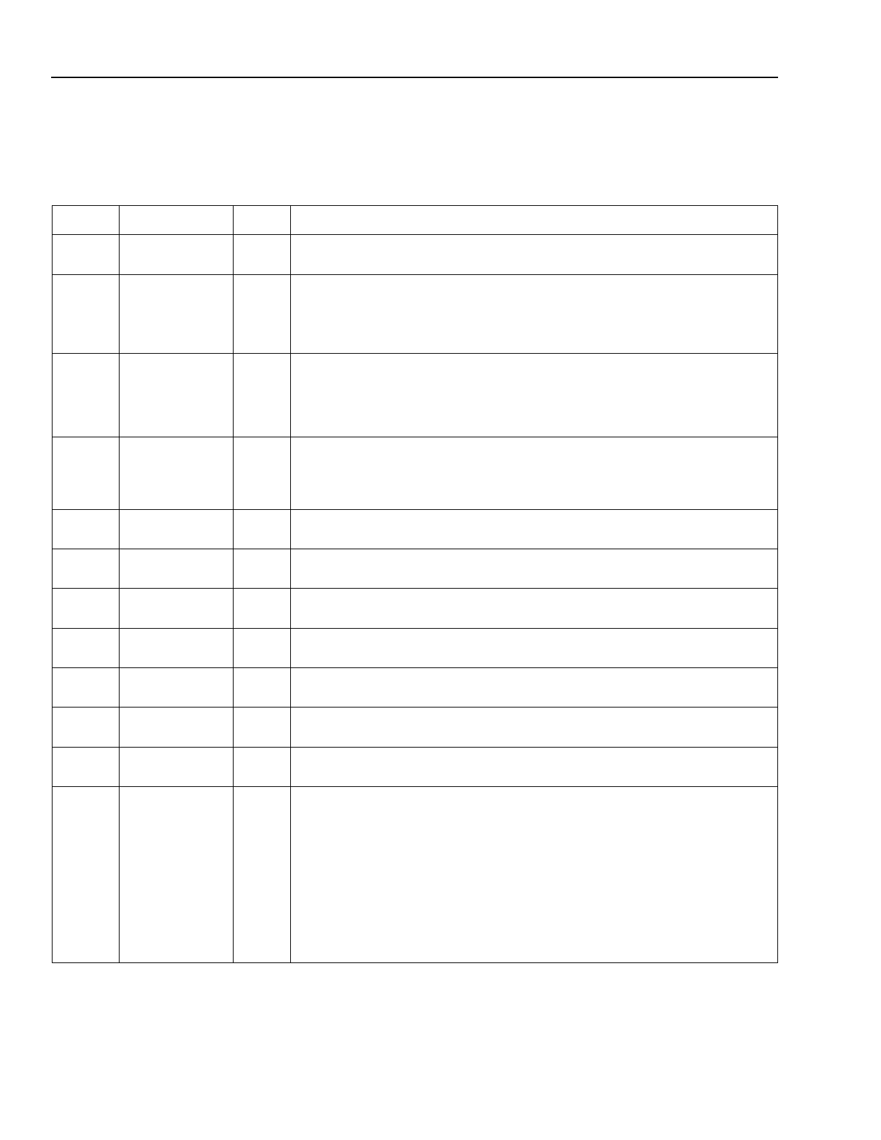
Table 1. Pin Descriptions
Pin
Symbol
Type*
Name/Description
117
CLKS
Id XCLK Select. This pin selects either a 16x rate clock for XCLK (CLKS = 0)
or a primary line rate clock for XCLK (CLKS = 1).
116
CLKM
Id XCLK Mode. This pin must be set appropriately when using a primary line
rate clock for XCLK.
CEPT: CLKM = 1.
DS1: CLKM = 0.
118
CMODE
Id Chip Mode. This pin sets the chip mode for either direct logic mode or
microprocessor mode.
128, 132
25, 29,
56, 60,
97, 101
129, 28,
57, 100
GNDX[1—4]
TTIP[1—4]
Microprocessor: CMODE = 1.
Direct Logic: CMODE = 0.
P Ground Reference for Line Drivers.
O Transmit Bipolar Tip. Positive bipolar transmit data to the analog line
interface.
130, 27,
58, 99
131, 26,
59, 98
VDDX[1—4]
TRING[1—4]
P Power Supply for Line Drivers. The TLIU04C1 device requires a 5 V ± 5%
power supply on these pins.
O Transmit Bipolar Ring. Negative bipolar transmit data to the analog line
interface.
133, 24,
61, 96
134, 23,
62, 95
135, 22,
63, 94
136, 21,
64, 93
VDDA[1—4]
RTIP[1—4]
RRING[1—4]
GNDA[1—4]
P Power Supply for Analog Circuitry. The TLIU04C1 device requires a 5 V
± 5% power supply on these pins.
I Receive Bipolar Tip. Positive bipolar receive data from the analog line
interface.
I Receive Bipolar Ring. Negative bipolar receive data from the analog line
interface.
P Ground Reference for Analog Circuitry.
137, 20, RND/BPV[1—4] O Receive Negative Data. When in dual-rail (DUAL = 1: register 5, bit 4)
65, 92
clock recovery mode (CDR = 1: register 5, bit 0), this signal is the received
negative NRZ data to the terminal equipment. When in data slicing mode
(CDR = 0), this signal is the raw sliced negative data of the front end.
Bipolar Violation. When in single-rail (DUAL = 0: register 5, bit 4) clock
recovery mode (CDR = 1: register 5, bit 0), and CODE = 1 (register 5, bit 3),
this signal is asserted high to indicate the occurrence of a code violation in
the receive data stream. A code violation is a bipolar violation that is not
part of a zero substitution code. If CODE = 0, this signal is asserted to
indicate the occurrence of a bipolar violation in the received data.
* I = input, O = output, Iu indicates an input with internal pull-up; Id indicates an input with internal pull-down, P = power. Resistance value of all
internal pull-ups or pull-downs is 50 kΩ, unless otherwise specified.
10
Lucent Technologies Inc.
Share Link: 