FX469 データシートの表示(PDF) - CML Microsystems Plc
部品番号
コンポーネント説明
メーカー
FX469 Datasheet PDF : 9 Pages
| |||
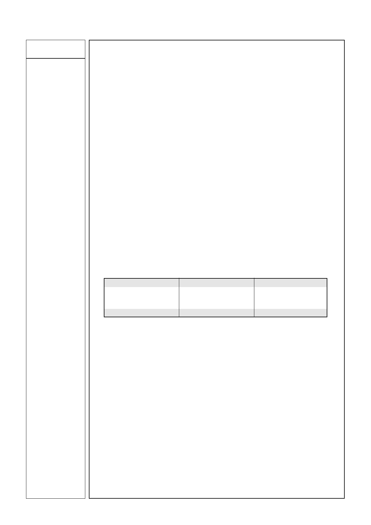
Pin Number Function
FX469
DW LG/LS J/P6
11 13 12 Unclocked Data O/P: The recovered asynchronous serial data output from the receiver.
12 14 13 Clocked Data O/P: The recovered synchronous serial data output from the receiver.
Data is latched out by the recovered clock, available at the “Rx Sync O/P,” (See Figure 5).
13 15 14 Carrier Detect O/P: When an FFSK signal is being received this output is a logic ‘1.’
14 16 15 Rx Signal I/P: The FFSK signal input for the receiver. This input should be coupled via a
capacitor, C3.
15 18 17 Rx Sync O/P: A flywheel squarewave output. This clock will synchronize to incoming Rx
FFSK data (See Figure 5).
16 19 16 1200/2400 Baud Select: A logic ‘1’ on this pin selects the 1200 baud option.
Tone frequencies are: one cycle of 1200Hz represents a logic ‘1,’ one-and-a-half cycles of
1800Hz represents a logic ‘0.’ A logic ‘0’ on this pin selects the 2400 baud option.
Tone frequencies are: one-half cycle of 1200Hz represents a logic ‘1,’ one cycle of 2400Hz
represents a logic ‘0.’ This function is also used, in part, to select the 4800 baud option. This
pin has an internal 1MW pullup resistor.
Operational Data Rate Configurations are illustrated in the table below.
Xtal/Clock Frequency
Clock Rate pin
1200/2400 Select pin
4800 Select pin
Baud Rate
1.008MHz
0
0
1
0
0
0
1200
2400
4.032MHz
1
1
1
1
0
0
0
0
1
1200 2400 4800
17 20 18 4800 Baud Select: A logic ‘1’ on this pin combined with a logic ‘0’ on the 1200/2400 Baud
Select pin will select the 4800 option (1MW pulldown resistor).
Tone frequencies are: one-half cycle of 2400Hz represents a logic ‘1,’ one cycle of 4800Hz
represents a logic ‘0.’ This state can only be achieved using a 4.032MHz Xtal input.
18 21 19 Clock Rate: A logic input to select and allow the use of either a 1.008MHz or 4.032MHz
Xtal/clock. Logic ‘1’ = 4.032MHz, logic ‘0’ = 1.008MHz. This input has an internal pulldown
resistor (1.008MHz).
19 22 20 Carrier Detect Time Constant : Part of the carrier detect integration function. The value of
C connected to this pin will affect the carrier detect response time and hence noise
4
performance (See Figure 2, Note 3).
20 24 22 VDD: Positive supply rail. A single 5-volt supply is required.
4, 6, 17, 4,
23 21
No internal connection, do not use.
3
Share Link: 