CMX269A データシートの表示(PDF) - MX-COM Inc
部品番号
コンポーネント説明
メーカー
CMX269A Datasheet PDF : 18 Pages
| |||
1200/2400/4800bps MSK Modem
5
CMX469A PRELIMINARY INFORMATION
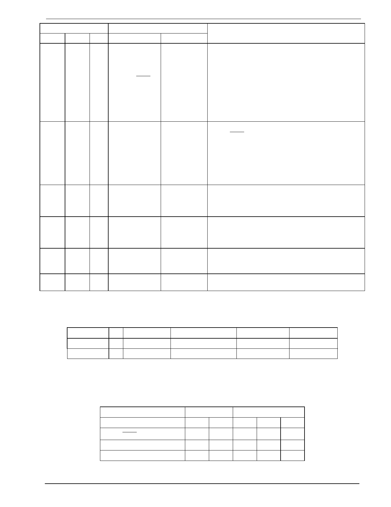
Pin No.
E2
P6 D3
Signal
Name
Type
Description
A logic ‘1’ on this pin selects the 1200bps option.
Tone frequencies are: one cycle of 1200Hz
represents a logic ‘1’, one-and-a-half cycles of
1800Hz represents a logic ‘0’.
19
16
16
1200 / 2400
BPS Select
input
A logic ‘0’ on this pin selects the 2400bps option.
Tone frequencies are: one-half cycle of 1200Hz
represents a logic ‘1’, one cycle of 2400Hz
represents a logic ‘0’. This pin has an internal 1MΩ
pull-up resistor. Operational Data Rate
Configurations are illustrated in Table 3.
20
18 17
4800
BPS Select
input
A logic '1' on this pin combined with a logic '0' on the
1200 / 2400 BPS Select pin will select the 4800
option (1MΩ pulldown resistor). Tone frequencies
are: one-half cycle of 2400Hz represents a logic '1',
one full cycle of 4800Hz represents a logic '0'. This
state can only be achieved using a 4.032MHz Xtal
input. Operational Data Rate Configurations are
illustrated in Table 3.
21
19 18 Clock Rate
input
A logic input to select and allow the use of either a
1.008MHz or 4.032MHz Xtal/clock. Logic ‘1’ =
4.032MHz, logic ‘0’ = 1.008MHz. This input has an
internal pulldown resistor (1.008MHz).
Part of the carrier detect integration function. The
22
20
19
Carrier Detect
Time Constant
bi-directional
value of C4 connected to this pin will affect the
carrier detect response time and therefore the noise
performance.
24
22 20
VDD
power
Positive supply. A single 2.7 to 5.0 volt supply is
required. This pin should be bypassed to VSS by a
capacitor (C5).
4, 6,
17, 23
4, 21
No internal connection, do not use.
Table 1: Signal List
RX Enable = RX Function Clock Data Output Carrier Detect Rx Sync Out
1
=
Enabled
Enabled
* Enabled
Enabled
0
= Powersave
0
1 or 0
1 or 0
* After enabling the receiver, a time of at least 8 bit periods, plus 2ms, should be allowed for
the Carrier Detect circuit to stabilize and provide a valid output.
Table 2: RX Enable Control Functions
XTAL/CLOCK Frequency
Clock Rate pin
1200 / 2400 Select Pin
4800 Select Pin
Data Rate (bps)
1.008MHz
0
0
1
0
0
0
1200 2400
4.032MHz
1
1
1
1
0
0
0
0
1
1200 2400 4800
Table 3: Operational Data Rate Configuration
©1999 MX-COM, Inc.
www.mxcom.com tel: 800 638 5577 336 744 5050 fax: 336 744 5054
Doc. # 20480191.002
4800 Bethania Station Road, Winston-Salem, NC 27105-1201 USA
All trademarks and service marks are held by their respective companies.
Share Link: 