MX469D3 データシートの表示(PDF) - MX-COM Inc
部品番号
コンポーネント説明
メーカー
MX469D3 Datasheet PDF : 17 Pages
| |||
1200/2400/4800bps MSK Modem
10
5. Application
MX469
5.1 Synchronous Modem Design Considerations
The MX469 is an easily applied data pump, which can be used with many protocols. Because it is an MSK, or
minimum shift keying, modem, it achieves a more noise resistant, higher data rate in a narrower bandwidth
than other FSK (frequency shift keying) modems. This characteristic is especially important for wireless
applications because it fundamentally determines the bandwidth of RF transmissions, which are strictly limited
and controlled by regulatory agencies. Using MSK signaling, the MX469 data modem can achieve a 2400bps
data rate within the typical 300-3000 Hz voice band of many common radios.
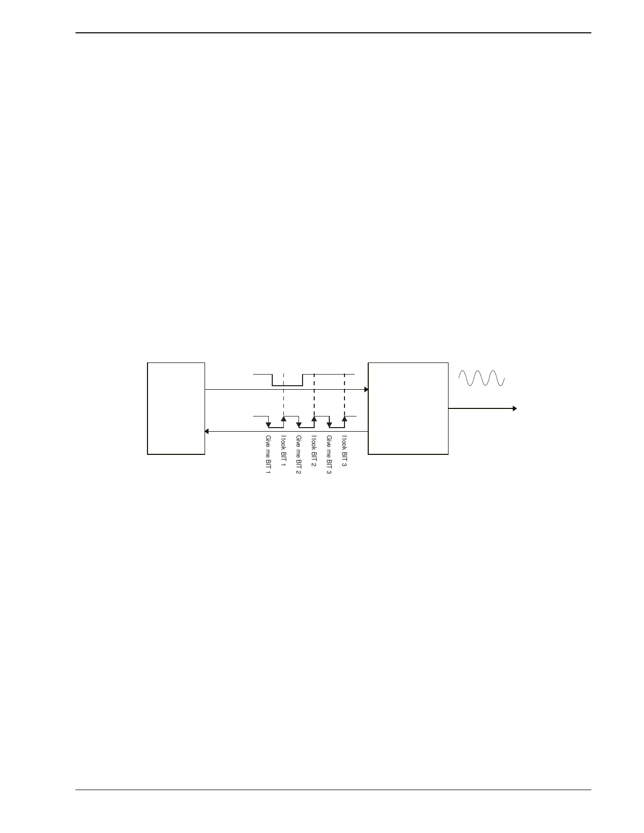
In order to achieve this advantage, an MSK modem must precisely control the bit rate and timing of the
modulated Tx output signal bits. This control is asserted by the MSK modem with a data clock signal, which
is output, by the modem to pace the Tx data source (e.g. a microcontroller). The data clock signal, in effect,
indicates when the Tx data source should provide the next Tx data bit to the modem. See Figure 9. Because
this type of interface involves the use of a modem generated bit clock signal to control the timing of when new
Tx data bits must be supplied from the data source, the interface is called synchronous.
Another characteristic of a synchronous modem is that, to receive data, it must first learn the data bit timing of
the Rx signal stream before it can accurately demodulate Rx data bits. Accordingly, a synchronous modem
undergoes a period of training or synchronization when it first begins to receive a stream of MSK modulated
signal. During this initial receive phase, the received signal is evaluated over several bit times as the modem
‘locks on’ and achieves proper receive synchronization. The training sequence, called a preamble, is a
specific data pattern which must be added to the ‘front’ of a transmit data stream with the start of each new
transmission. A specific preamble data pattern (e.g. 16 bits of alternating 0,1,0,1… for the MX469) is used to
optimize the training accuracy while minimizing the number of preamble bits required.
Tx data
Data Bit Tx
Source
(e.g. µC)
DATA: 0 1 1
01 1
MSK Modem
Transmitting
MSK Tx Out
Tx SYNC
(data clock)
Figure 9: Synchronous Transmit Operation
Non-synchronous or asynchronous interfaces are commonly found in wired applications which do not have
the bandwidth efficiency requirements of wireless systems. A well known example is the serial port of a
personal computer which can transmit a 1200 bps (or faster) data signal over a single Tx signal without using
an additional data clock signal to control the precise rate and timing of data bits being transmitted to a typical
telephone line data modem. Popular modem standards such as Bell 202 and v.23 use FSK signaling to pass
such asynchronous serial port data signals over telephone systems.
Another aspect of asynchronous interfaces and modems is that they can carry data streams which are not at
the exact, nominal data rate. For example, a 1200 bps FSK modem will typically operate properly when
supplied with transmit data streams of 1201 bps or 1199 bps.
Because of the differences in synchronous and asynchronous interfaces, they cannot successfully operate if
directly connected. In other words, a personal computer’s RS232 serial port cannot directly interface to an
MSK modem. This is because:
The asynchronous interface may provide data bits too fast or too slow compared to the precise rate
required for MSK signaling (a bit rate, or pacing, incompatibility).
The timing of each specific data bit presented by an asynchronous interface will not be aligned with the
precise bit timing required for MSK signaling (a bit timing incompatibility).
Synchronous and asynchronous interface can be successfully interfaced for applications requiring the
advantages of both. This typically involves the use of data buffering and retiming circuits to resolve the timing
and pacing issues.
1998 MX-COM, Inc.
www.mxcom.com Tel: 800 638 5577 336 744 5050 Fax: 336 744 5054
Doc. # 20480081.010
4800 Bethania Station Road, Winston-Salem, NC 27105-1201 USA
All trademarks and service marks are held by their respective companies.
Share Link: 