HS-1212RH データシートの表示(PDF) - Intersil
部品番号
コンポーネント説明
メーカー
HS-1212RH Datasheet PDF : 9 Pages
| |||
HS-1212RH
Application Information
HS-1212RH Advantages
The HS-1212RH features a novel design which allows the
user to select from three closed loop gains, without any
external components. The result is a more flexible product,
fewer part types in inventory, and more efficient use of board
space. Implementing a dual, gain of 2, cable driver with this
IC eliminates the four gain setting resistors, which frees up
board space for termination resistors.
Like most newer high performance amplifiers, the
HS-1212RH is a current feedback amplifier (CFA). CFAs
offer high bandwidth and slew rate at low supply currents,
but can be difficult to use because of their sensitivity to
feedback capacitance and parasitics on the inverting input
(summing node). The HS-1212RH eliminates these
concerns by bringing the gain setting resistors on-chip. This
yields the optimum placement and value of the feedback
resistor, while minimizing feedback and summing node
parasitics. Because there is no access to the summing node,
the PCB parasitics do not impact performance at gains of +2
or -1 (see “Unity Gain Considerations” for discussion of
parasitic impact on unity gain performance).
The HS-1212RH’s closed loop gain implementation provides
better gain accuracy, lower offset and output impedance,
and better distortion compared with open loop buffers.
Closed Loop Gain Selection
This “buffer” operates in closed loop gains of -1, +1, or +2, with
gain selection accomplished via connections to the inputs.
Applying the input signal to +IN and floating -IN selects a gain
of +1 (see next section for layout caveats), while grounding -IN
selects a gain of +2. A gain of -1 is obtained by applying the
input signal to -IN with +IN grounded through a 50Ω resistor.
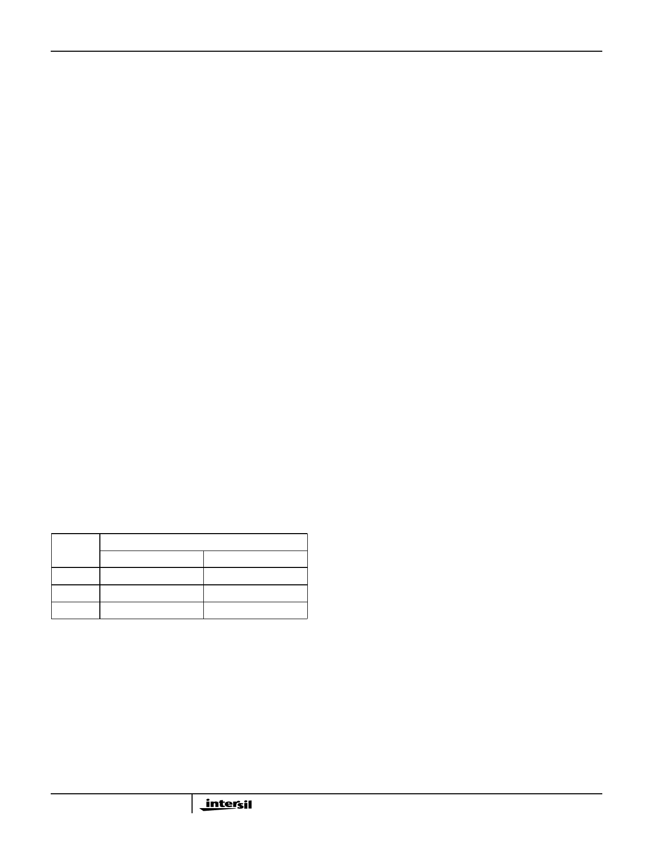
The table below summarizes these connections:
GAIN
(ACL)
-1
+1
+2
CONNECTIONS
+INPUT
-INPUT
50Ω to GND
Input
Input
NC (Floating)
Input
GND
Unity Gain Considerations
Unity gain selection is accomplished by floating the -Input of
the HS-1212RH. Anything that tends to short the -Input to
GND, such as stray capacitance at high frequencies, will
cause the amplifier gain to increase toward a gain of +2. The
result is excessive high frequency peaking, and possible
instability. Even the minimal amount of capacitance
associated with attaching the -Input lead to the PCB results
in approximately 6dB of gain peaking. At a minimum this
requires due care to ensure the minimum capacitance at the
-Input connection.
Table 1 lists five alternate methods for configuring the
HS-1212RH as a unity gain buffer, and the corresponding
performance. The implementations vary in complexity and
involve performance trade-offs. The easiest approach to
implement is simply shorting the two input pins together,
and applying the input signal to this common node. The
amplifier bandwidth decreases from 430MHz to 280MHz,
but excellent gain flatness is the benefit. A drawback to this
approach is that the amplifier input noise voltage and input
offset voltage terms see a gain of +2, resulting in higher
noise and output offset voltages. Alternately, a 100pF
capacitor between the inputs shorts them only at high
frequencies, which prevents the increased output offset
voltage but delivers less gain flatness.
Another straightforward approach is to add a 620Ω resistor
in series with the amplifier’s positive input. This resistor and
the HS-1212RH input capacitance form a low pass filter
which rolls off the signal bandwidth before gain peaking
occurs. This configuration was employed to obtain the data
sheet AC and transient parameters for a gain of +1.
Pulse Overshoot
The HS-1212RH utilizes a quasi-complementary output stage
to achieve high output current while minimizing quiescent
supply current. In this approach, a composite device replaces
the traditional PNP pulldown transistor. The composite device
switches modes after crossing 0V, resulting in added distortion
for signals swinging below ground, and an increased overshoot
on the negative portion of the output waveform (see Figure 6,
Figure 9, and Figure 12). This overshoot isn’t present for small
bipolar signals (see Figure 4, Figure 7, and Figure 10) or large
positive signals (see Figure 5, Figure 8 and Figure 11).
PC Board Layout
This amplifier’s frequency response depends greatly on the
care taken in designing the PC board (PCB). The use of low
inductance components such as chip resistors and chip
capacitors is strongly recommended, while a solid
ground plane is a must!
Attention should be given to decoupling the power supplies.
A large value (10µF) tantalum in parallel with a small value
(0.1µF) chip capacitor works well in most cases.
2
Share Link: 