HS-1145RH(1999) データシートの表示(PDF) - Intersil
部品番号
コンポーネント説明
メーカー
HS-1145RH
(Rev.:1999)
(Rev.:1999)
Intersil

HS-1145RH Datasheet PDF : 9 Pages
| |||
HS-1145RH
Application Information
Optimum Feedback Resistor
Although a current feedback amplifier’s bandwidth
dependency on closed loop gain isn’t as severe as that of a
voltage feedback amplifier, there can be an appreciable
decrease in bandwidth at higher gains. This decrease may
be minimized by taking advantage of the current feedback
amplifier’s unique relationship between bandwidth and RF.
All current feedback amplifiers require a feedback resistor,
even for unity gain applications, and RF, in conjunction with
the internal compensation capacitor, sets the dominant pole
of the frequency response. Thus, the amplifier’s bandwidth is
inversely proportional to RF. The HS-1145RH design is
optimized for RF = 510Ω at a gain of +2. Decreasing RF
decreases stability, resulting in excessive peaking and
overshoot (Note: Capacitive feedback will cause the same
problems due to the feedback impedance decrease at higher
frequencies). At higher gains, however, the amplifier is more
stable so RF can be decreased in a trade-off of stability for
bandwidth.
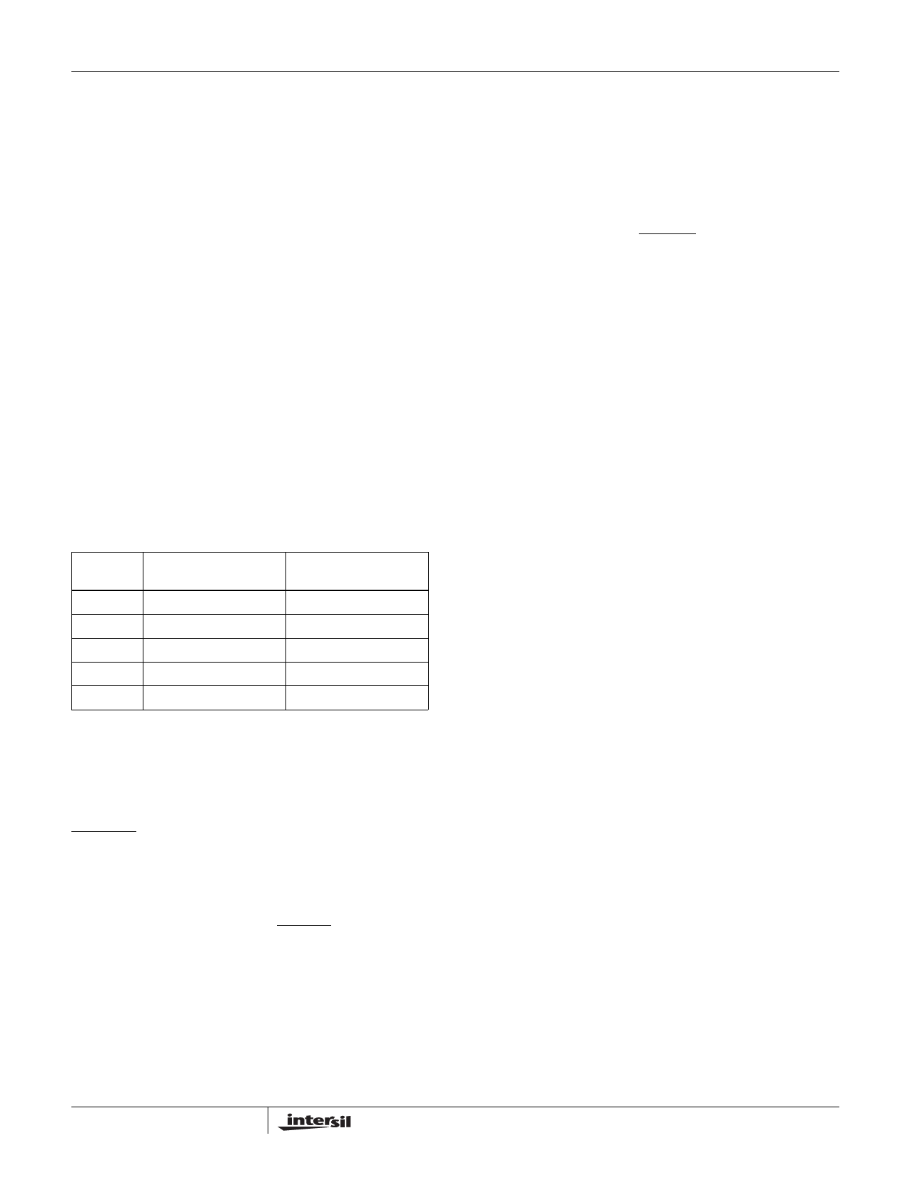
The table below lists recommended RF values for various
gains, and the expected bandwidth. For a gain of +1, a
resistor (+RS) in series with +IN is required to reduce gain
peaking and increase stability.
GAIN
(ACL)
-1
+1
+2
+5
+10
RF (Ω)
425
510 (+RS = 510Ω)
510
200
180
BANDWIDTH
(MHz)
300
270
330
300
130
Non-Inverting Input Source Impedance
For best operation, the DC source impedance seen by the
non-inverting input should be ≥50Ω. This is especially
important in inverting gain configurations where the non-
inverting input would normally be connected directly to GND.
DISABLE Input TTL Compatibility
The HS-1145RH derives an internal GND reference for the
digital circuitry as long as the power supplies are symmetrical
about GND. With symmetrical supplies the digital switching
threshold (VTH = (VIH + VIL)/2 = (2.0 + 0.8)/2) is 1.4V, which
ensures the TTL compatibility of the DISABLE input. If
asymmetrical supplies (e.g., +10V, 0V) are utilized, the
switching threshold becomes:
VTH = V-----+----2-+----V------ + 1.4V
and the VIH and VIL levels will be VTH ± 0.6V, respectively.
Optional GND Pad (Die Use Only) for TTL
Compatibility
The die version of the HS-1145RH provides the user with a
GND pad for setting the disable circuitry GND reference.
With symmetrical supplies the GND pad may be left
unconnected, or tied directly to GND. If asymmetrical
supplies (e.g., +10V, 0V) are utilized, and TTL compatibility
is desired, die users must connect the GND pad to GND.
With an external GND, the DISABLE input is TTL compatible
regardless of supply voltage utilized.
Pulse Undershoot and Asymmetrical Slew Rates
The HS-1145RH utilizes a quasi-complementary output
stage to achieve high output current while minimizing
quiescent supply current. In this approach, a composite
device replaces the traditional PNP pulldown transistor. The
composite device switches modes after crossing 0V,
resulting in added distortion for signals swinging below
ground, and an increased undershoot on the negative
portion of the output waveform (See Figures 5, 8, and 11).
This undershoot isn’t present for small bipolar signals, or
large positive signals. Another artifact of the composite
device is asymmetrical slew rates for output signals with a
negative voltage component. The slew rate degrades as the
output signal crosses through 0V (See Figures 5, 8, and 11),
resulting in a slower overall negative slew rate. Positive only
signals have symmetrical slew rates as illustrated in the
large signal positive pulse response graphs (See Figures 4,
7, and 10).
PC Board Layout
This amplifier’s frequency response depends greatly on the
care taken in designing the PC board. The use of low
inductance components such as chip resistors and chip
capacitors is strongly recommended, while a solid
ground plane is a must!
Attention should be given to decoupling the power supplies.
A large value (10µF) tantalum in parallel with a small value
(0.1µF) chip capacitor works well in most cases.
Terminated microstrip signal lines are recommended at the
device’s input and output connections. Capacitance,
parasitic or planned, connected to the output must be
minimized, or isolated as discussed in the next section.
Care must also be taken to minimize the capacitance to
ground at the amplifier’s inverting input (-IN), as this
capacitance causes gain peaking, pulse overshoot, and if
large enough, instability. To reduce this capacitance, the
designer should remove the ground plane under traces
connected to -IN, and keep connections to -IN as short as
possible.
An example of a good high frequency layout is the
Evaluation Board shown in Figure 2.
2
Share Link: