LT1620 データシートの表示(PDF) - Linear Technology
部品番号
コンポーネント説明
メーカー
LT1620 Datasheet PDF : 12 Pages
| |||
LT1620/LT1621
PI FU CTIO S
input (across external sense resistor) equal to (VCC –
VPROG)/10. Input voltage range is VCC to (VCC – 1.25V).
AVG2: Sense Amplifier AV = – 20 Output and Comparator
Positive Input. Used as integration node for end-of-cycle
determination flag. Integration time constant is calculated
using 5kΩ typical output impedance.
PROG2: Comparator Negative Input. Program node for
end-of-cycle determination typically used during voltage
mode operation. The comparator threshold is reached
when the current sense amplifier differential input voltage
equals (VCC – VPROG2)/20. Input voltage range is (VCC –
0.15V) to (VCC – 2.5V).
GND: Ground Reference.
MODE: Comparator Open Collector Output. Output is logic
low when magnitude of current sense amplifier differential
input voltage is less than (VCC – VPROG2)/20.
IOUT: Transconductance Amplifier Output. In typical appli-
cation, IOUT sinks current from current-setting node on
companion PWM controller IC, facilitating current mode
loop control.
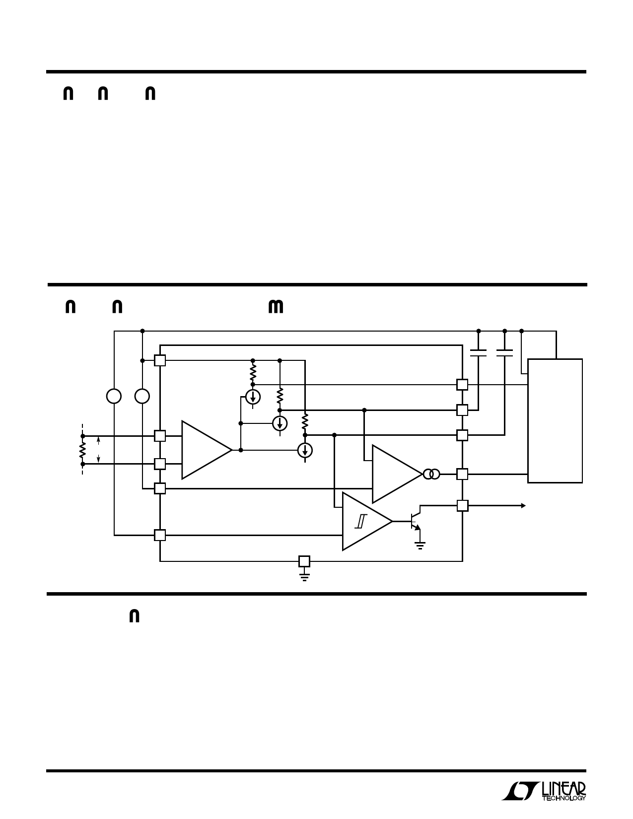
W
FUNCTIONAL BLOCK DIAGRA
5V
+–
CURRENT
SENSE
VID
RESISTOR
VCC
+–
500Ω
2.5k
IN+ +
SENSE
IN–
AMPLIFIER
–
PROG
5k
+
PROG2*
*AVAILABLE IN THE LT1620GN ONLY
–
GND
(×1 GAIN) SENSE
(×10 GAIN) AVG
(×20 GAIN) AVG2*
+
gm
–
IOUT
MODE*
LT1620/21 • FBD
INTVCC
SENSE+
SENSE–
PWM
CONTROLLER
ITH
END-OF-CYCLE
(ACTIVE LOW)
U
OPERATION (Refer to the Functional Block Diagram)
Current Sense Amplifier
The current sense amplifier is a multiple output voltage
amplifier with an operational input common mode range
from 0V to 32V. The amplifier generates scaled output
voltages at the SENSE, AVG and AVG2 (available in
LT1620GN) pins. These output signal voltages are refer-
enced to the VCC supply by pulling signal current through
internal VCC referred resistors.
The first output (SENSE) is a unity gain, level-shifted repre-
sentation of the input signal (IN+ – IN–). In typical PWM/
charger type applications, this output is used to drive the
current sense amplifier of the mated PWM controller IC.
The other two outputs (AVG and AVG2) are internally
connected to a transconductance amplifier and compara-
tor, respectively. The AVG output yields a gain of 10, and
the AVG2 output provides a gain of 20. These pins are
4
Share Link: 