MC14LC5003 データシートの表示(PDF) - Motorola => Freescale
部品番号
コンポーネント説明
メーカー
MC14LC5003 Datasheet PDF : 17 Pages
| |||
FUNCTIONAL DESCRIPTION
The MC14LC5002/5003/5004 have essentially two sections
which operate asynchronously from each other; the data input
and storage section and the LCD drive section. The LCD drive
and timing is derived from the oscillator, while the data input
and storage is controlled by the Data In (Din), Data Clock
(DCLK), Address (A0, A1, A2), and Enable (ENB) pins.
Data is shifted serially into the 128-bit shift register and ar-
ranged into four consecutive blocks of 32 parallel data bits. A
time-multiplex of the four backplane drivers is made (each
backplane driver becoming active then inactive one after an-
other) and, at the start of each backplane active period, the
corresponding block of 32 bits is made available at the front-
plane drivers. A high input to a plane driver turns the driver
on, and a low input turns the driver off.
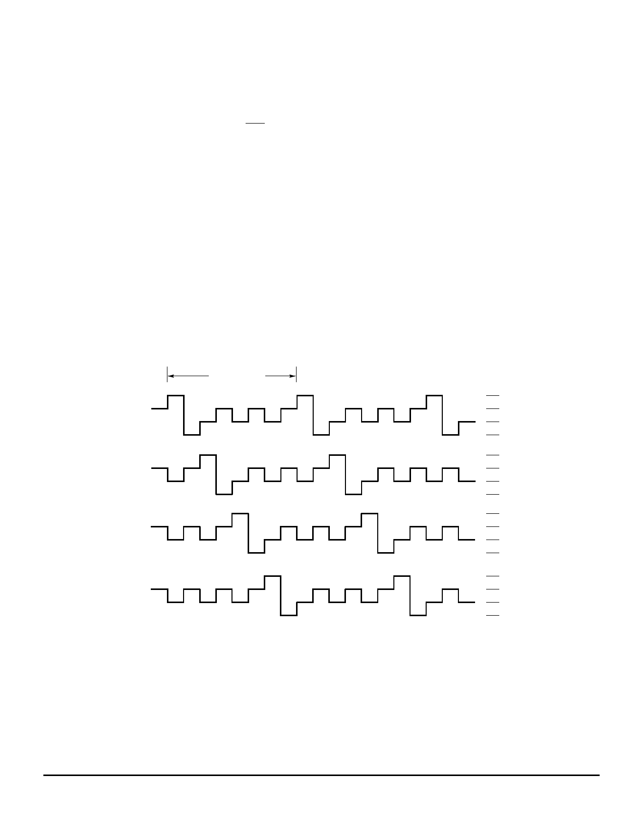
Figure 4 shows the sequence of backplanes. Figure 5 shows
the possible configurations of the frontplanes relative to the
backplanes.When a backplane driver is on, its output switches
from VLCD to 0 V, and when it is off, it switches from 1/3 VLCD
to 2/3 VLCD. When a frontplane driver is on, its
output switches from 0 V to VLCD, and when it is off, it switches
from 2/3 VLCD to 1/3 VLCD.
The LCD drive and timing section provides the multiplex sig-
nals and backplane driver input signals and formats the front-
plane and backplane waveforms.
The address pins are used to uniquely distinguish LCD driver
from any other chips on the same bus and to define LCD driver
as the “master” in the system. There must be one master in any
system.
The enable pin may be used as a third control line in the
communication bus. It may be used to define the moment
when the data is latched. If not used, then the data is latched
after 128 bits of data have been received.
TIME FRAME
BP1
BP2
BP3
BP4
Figure 4. Backplane Sequence
VLCD
2/3 (VLCD)
1/3 (VLCD)
0V
VLCD
2/3 (VLCD)
1/3 (VLCD)
0V
VLCD
2/3 (VLCD)
1/3 (VLCD)
0V
VLCD
2/3 (VLCD)
1/3 (VLCD)
0V
MOTOROLA
MC14LC5002 • MC14LC5003 • MC14LC5004
3–9
Share Link: 