MXED202 データシートの表示(PDF) - Clare Inc => IXYS
部品番号
コンポーネント説明
メーカー
MXED202 Datasheet PDF : 16 Pages
| |||
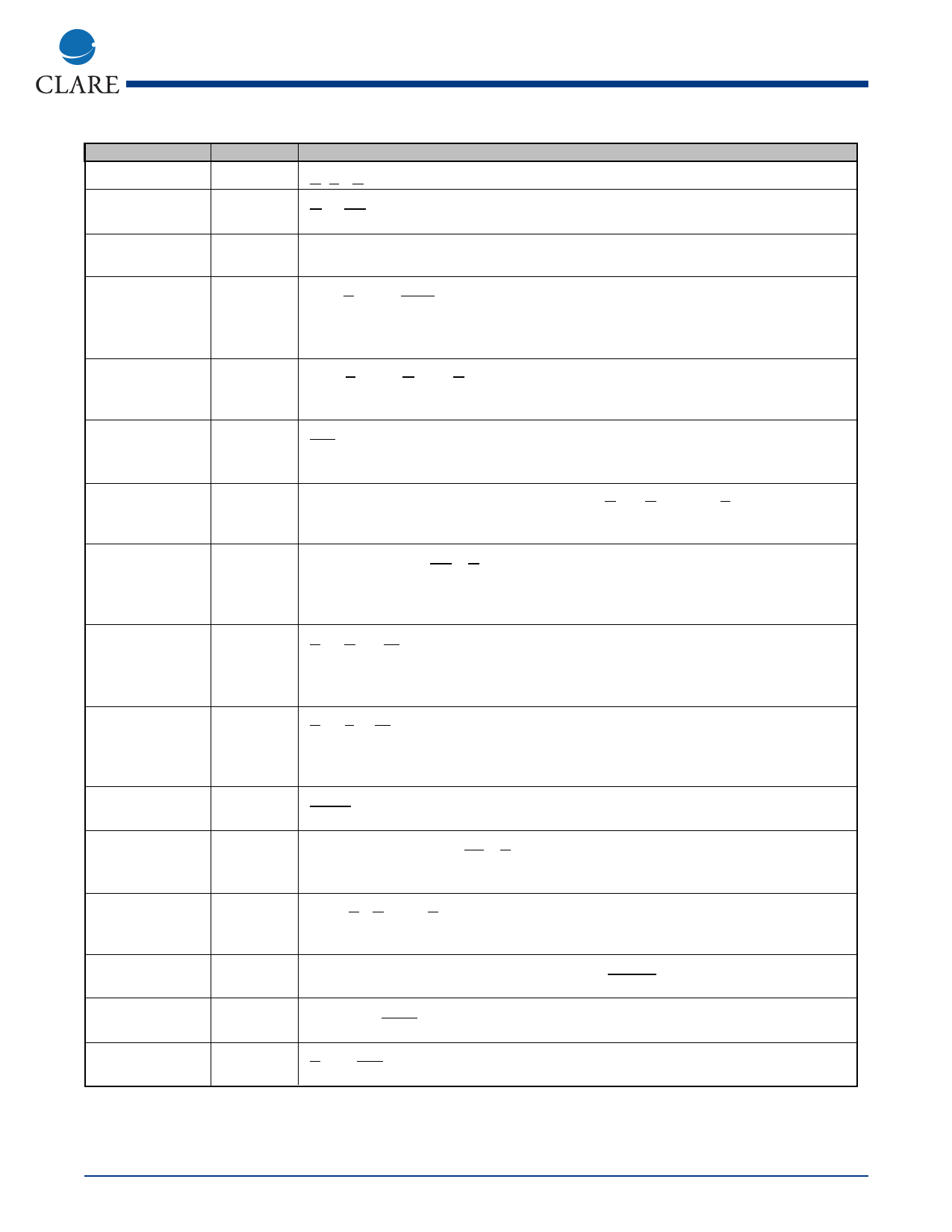
PIN LIST
Name
RTN
GND
VCC
VMAX
VOH
[Page 12]
INV
[Page 12]
DRV
[Page 12]
SHR
SRIN
SLIN
DUAL
CLK
PCB
[Pages 9-11]
MONO
[Pages 9-11]
MOD
[Pages 9-11]
S128
Preliminary
MXED202
I/O/A
I
I
I
I
I/O/A
I
I
I
I/O
I/O
I
I
I
I
I
I
Description
ReTurN for all display current. (Low impedance ground connection, typically)
GrouND, the negative return for all chip current and the digital logic "zero" refer
ence level.
The logic voltage positive supply. MXED202 logic operates between VCC and
VSS. Digital inputs should not exceed VCC, VSS
This Voltage MAXimum is the highest positive power supply voltage present on
the chip, and supplies the display panel precharge current either directly or at
derived voltage VOH. Inputs to the chip should not exceed VMAX to avoid for
ward biasing substrate diodes.
Row Voltage Output High supply. This pin is normally connected to an external
power supply pin VMAX with bypass capacitor, and to pin DRV. Alternatively, an
internal amplifier can generate VOH from an input voltage DRV.
INVerting input to Voltage Regulator Op Amp, to which an input Resistor RI and
feedback Resistor RF may be connected to develop VOH from VDRV; see DRV
pin.
When not connected to VOH and VMAX, a Drive Reference Voltage >1V can be
connected to the DRV pin.Note: If VDRV <0.3V, all row circuitry is powered
down.
Active high static SHift Right control input: When SHR=1, the token bit travels
from R0 to R127, with SRIN being the token input, SLIN the token output. When
SHR=0, the token bit travels from R127 to R0, with SLIN being the token input,
SRIN the token output. SHR should always be driven to the desired logic level.
Shift Right INput. This bi-directional pin is the token input when SHR is high, and
the token output (for synchronization or cascading) when SHR is low. When con
figured as an input, this pin should always be driven. Normally low, SRIN should
be driven high once per frame to enter the token into the shift register.
Shift Left INput. This bi-directional pin is the token input when SHR is low, and
the token output (for synchron- ization or cascading) when SHR is high. When
configured as an input, this pin should always be driven. Normally low, SLIN
should be driven high once per frame to enter the token into the shift register.
DUAL tokens are seeded into the first and middle shift register cells from SRIN
or SLIN when DUAL is static active high. When low, a single token is active.
The rising edge of the CLocK input shifts the token along the internal shift regis
ter to activate successive rows. The display Row Scan Rate is the CLK frequen
cy times the number of tokens.
If the PreCharge Bar input is low on the rising edge of CLK, all row outputs will
be switched to the same voltage (see MONO) to enable display panel precharg
ing until PCB returns high. Holding PCB high disables MXED202 precharge.
Enables MXED202 row driver precharge of MONOchromatic displays, if PCB=0.
The MONO input has no effect if PCB=1.
This input MODifies precharge timing
Select 128 row driver output mode when static active high. When low, 120 row
driver output mode is selected.
Rev. 2
www.clare.com
5
Share Link: 