CXA1645M データシートの表示(PDF) - Sony Semiconductor
部品番号
コンポーネント説明
メーカー
CXA1645M Datasheet PDF : 14 Pages
| |||
CXA1645P/M
Pin Description
Pin
No.
Symbol Pin voltage
1 GND1
0V∗
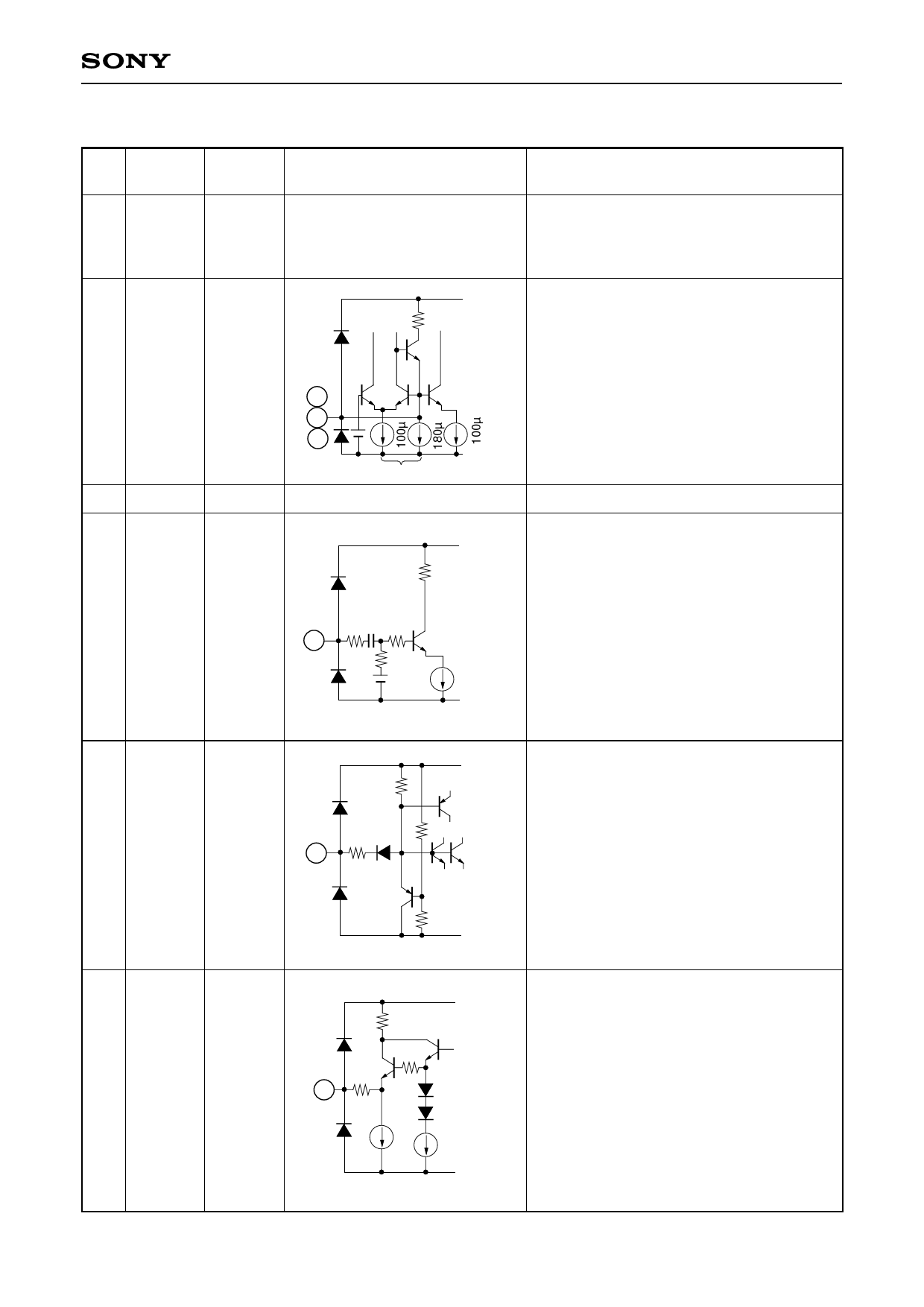
Equivalent circuit
VCC1
∗ Externally applied voltage
Description
Ground for all circuits other than RGB,
composite video and Y/C output circuits.
The leads to GND2 should be as short and
wide as possible.
2 RIN
3 GIN
4 BIN
Black level
when
clamped
2
2.0V
3
4
5 NC
Analog RGB signal inputs. Input
100%, = 1Vp-p (max.). To minimize clamp
error, input at as low impedance as
possible.
ICLP turns ON only in the burst flag period.
GND1
ICLP
NO CONNECTION
VCC1
6 SCIN
—
20P 20k
6
129 20k
Subcarrier input.
Input 0.4 to 0.5Vp-p sine wave or pulse.
Refer to Notes on Operation, Nos. 3 and 5.
2.5V
100µ
GND1
7 NPIN
1.7V
VCC1
80k
68k
7
3k
Pin for switching between NTSC and PAL
modes
NTSC: VCC, PAL: GND
32k
GND1
VCC1
8
BFOUT
H : 3.6V
L : 3.2V
8
129
25µ
25µ
GND1
BF pulse monitoring output. Incapable of
driving a 75Ω load.
–2–
Share Link: 