LF398 データシートの表示(PDF) - Philips Electronics
部品番号
コンポーネント説明
メーカー
LF398 Datasheet PDF : 5 Pages
| |||
Philips Semiconductors Linear Products
Sample-and-hold amplifiers
Product specification
LF198/LF298/LF398
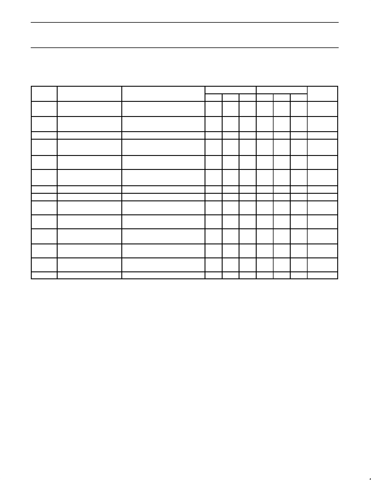
DC ELECTRICAL CHARACTERISTICS
Unless otherwise specified, the following conditions apply: unit is in “sample” mode; VS = ±15V; TJ = 25°C; -11.5V3 VIN ≤ +11.5V; CH=0.01µF;
and RL = 10kΩ. Logic reference voltage = 0V and logic voltage = 2.5V.
SYMBOL
PARAMETER
TEST CONDITIONS
LF198/LF298
LF398
Min Typ Max Min Typ Max
UNIT
VOS
Input offset voltage4
TJ=25°C
Full temperature range
1
3
5
2
7
mV
10
IBIAS
Input bias current4
TJ=25°C
Full temperature range
5
25
75
10 50
nA
100
Input impedance
Gain error
TJ=25°C
TJ=25°C, RL=10k
Full temperature range
1010
0.002 0.005
0.02
1010
Ω
0.004 0.01
%
0.02
Feedthrough attenuation
ratio at 1kHz
TJ=25°C, Ch=0.01µF
86 96
80 90
dB
Output impedance
TJ=25°C, “HOLD“ mode
Full temperature range
“HOLD“ step2
ICC
Supply current4
TJ=25°C, Ch=0.01µF, VOUT=0
TJ ≤ 25°C
Logic and logic reference
input current
TJ = 25°C
0.5 2
4
0.5 2.0
4.5 5.5
2
10
0.5 4
Ω
6
1.0 2.5
mV
4.5 6.5
mA
2
10
µA
Leakage current into hold
capacitor4
TJ=25°C, “HOLD“ mode
30 100
30 200
pA
tAC
Acquisition time to 0.1%
∆VOUT=10V, Ch=1000pF
Ch=0.01µF
4
20
Hold capacitor charging
current
VIN-VOUT=2V
5
4
µs
20
5
mA
Supply voltage rejection
ratio
VOUT=0
80 110
80 110
dB
Differential logic threshold
TJ=25°C
0.8 1.4 2.4 0.8 1.4 2.4
V
NOTES:
1. Unless otherwise specified, the following conditions apply. Unit is in “sample“ mode, VS=±15V, TJ=25°C, -11.5V ≤ VIN ≤ +11.5V, Ch = 0.01µF,
and RL = 10kΩ. Logic reference voltage = 0V and logic voltage = 2.5V.
2. Hold step is sensitive to stray capacitive coupling between input logic signals and the hold capacitor. 1pF, for instance, will create an
additional 0.5mV step with a 5V logic swing and a 0.01µF hold capacitor. Magnitude of the hold step is inversely proportional to hold
capacitor value.
3. Leakage current is measured at a junction temperature of 25°C. The effects of junction temperature rise due to power dissipation or elevated
ambient can be calculated by doubling the 25°C value for each 11°C increase in chip temperature. Leakage is guaranteed over full input
signal range.
4. The parameters are guaranteed over a supply voltage of ±5 to ±18V.
August 31, 1994
881
Share Link: 