OQ2541HP/C3 データシートの表示(PDF) - Philips Electronics
部品番号
コンポーネント説明
メーカー
OQ2541HP/C3 Datasheet PDF : 36 Pages
| |||
Philips Semiconductors
SDH/SONET data and clock recovery unit
STM1/4/16 OC3/12/48 GE
Product specification
OQ2541HP; OQ2541U
Reference frequency select
A reference clock signal of 19.44 or 38.88 MHz must be
connected to pins CREF and CREFQ. It should be noted
that the reference frequency should be either
39.0625 MHz or 19.53125 MHz in a Gigabit Ethernet
system. Pins DREF19 and DREF39 are used to select the
appropriate output frequency at frequency divider 2
(see Table 2).
To minimize the adverse influence of reference clock
crosstalk, a differential signal with an amplitude from
75 to 150 mV (p-p) is advised.
Since the reference clock is only used as an acquisition aid
for the PLL of the frequency window detector, the quality
of the reference clock (i.e. phase noise) is not important.
There is no phase noise specification imposed on the
reference clock generator and even frequency stability
may be in the order of 100 ppm. In general, most
inexpensive crystal based oscillators are suitable.
When the OQ2541 is used in an application with a fixed
reference clock frequency, it is best to connect the planes
of pins DREF19 and DREF39 with a short trace or a via to
the plane of pin GND or pin VEE. If a selectable reference
clock frequency is required in the application, the pins can
be controlled through low ohmic switching FETs,
e.g. BSH103 or equivalent (low RDSon).
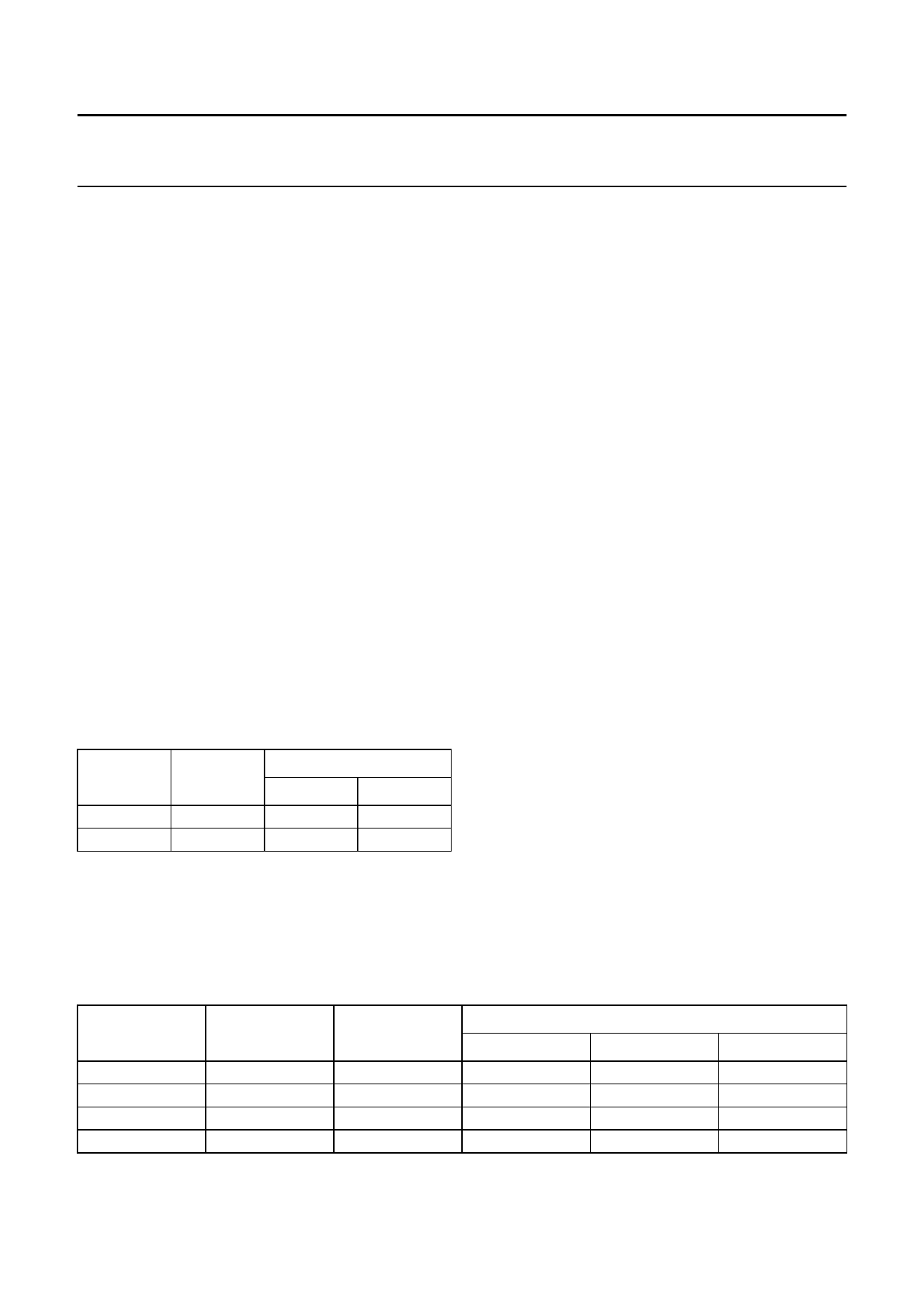
Table 2 Reference frequency selection
FREQUENC DIVISION
Y (MHz) FACTOR
38.88
64
19.44
128
LEVEL ON PIN
DREF19 DREF39
ground
VEE
VEE
VEE
STM mode selection
The VCRO has a very large tuning range. However, the
performance of the OQ2541 is optimized for SDH/SONET
bit rates.
Due to the nature of the PLL, the very wide tuning range is
a necessity for proper lock behaviour over the guaranteed
temperature range, aging and batch to batch spread.
Though it might seem that the OQ2541 is capable of
recovering other bit rates than SDH/SONET and Gigabit
Ethernet rates (STM1/OC3, STM4/OC12, STM16/OC48
and 1250 Mbits/s), the behaviour can not be guaranteed.
The required SDH/SONET bit rate is selected by
connecting pins DOUT155, DOUT622 and DOUT1250
to ground or to the supply voltage VEE (see Table 3):
• For STM16/OC48 (2488.32 Mbits/s) operation:
all three pins must be connected to ground
• For Gigabit Ethernet (1250 Mbits/s) operation:
pin DOUT1250 must be connected to VEE
• For STM4/OC12 (622.08 Mbits/s) operation:
pins DOUT1250 and DOUT622 must be connected to
VEE (the dividers are daisy chained)
• For STM1/OC3 (155,52 Mbits/s) operation:
all three pins must be connected to VEE.
The connections to VEE and ground carry a current of a few
milliamperes and should have low resistance and
inductance, so short printed-circuit board tracks are
recommended. In some cases a decoupling capacitor near
the selection pins can be necessary to provide a clean
return path for RF signals.
When the OQ2541 is used in an application with a fixed
data rate, it is best to connect the planes of
pins DOUT155, DOUT622 and DOUT1250 with a short
trace or a via to the plane of pin GND or pin VEE. If a
selectable reference clock frequency is required in the
application, the pins can be controlled through low-ohmic
switching FETs, e.g. BSH103 or equivalent (low RDSon).
Table 3 STM mode select
MODE
STM1/OC3
STM4/OC12
Gigabit Ethernet
STM16/OC48
BIT RATE
(Mbits/s)
155.52
622.08
1 250.00
2 488.32
DIVISION
FACTOR
16
4
2
1
DOUT155
VEE
ground
ground
ground
LEVEL ON PIN
DOUT622
VEE
VEE
ground
ground
DOUT1 250
VEE
VEE
VEE
ground
1999 May 27
10
Share Link: 