CXD3504R データシートの表示(PDF) - Sony Semiconductor
部品番号
コンポーネント説明
メーカー
CXD3504R Datasheet PDF : 12 Pages
| |||
CXD3504R
Description of Operation
1) The following describes only R, but the operation for G and B is the same.
SELRA:SELB = 0:0 R2IN → through → R1OUT
R1IN → delay → R2OUT
SELRA:SELB = 0:1 R2IN → delay → R1OUT
R1IN → through → R2OUT
SELRA:SELB = 1:0 R1IN → through → R1OUT
R2IN → delay → R2OUT
SELRA:SELB = 1:1 R1IN → delay → R1OUT
R2IN → through → R2OUT
However, POLSLA = 0
2) Be sure to set XCLR to "0" for a clock or more while HD is "1". (when HDSEL = 0) Also, input the HD signal
with a "0" period length of 6 clocks or more.
Very Little Signal Amplifier (VDD = 3.0 to 3.6V, Vss = 0V, Ta = –30 to +75°C)
Item
Symbol Min.
Typ. Max. Unit
High level input voltage
VIH
0.4
—
3.6
V
Low level input voltage
VIL
0
—
3.2
V
Input frequency
Input amplitude∗1
f
—
—
Vpp
0.4
—
80 MHz
—
V
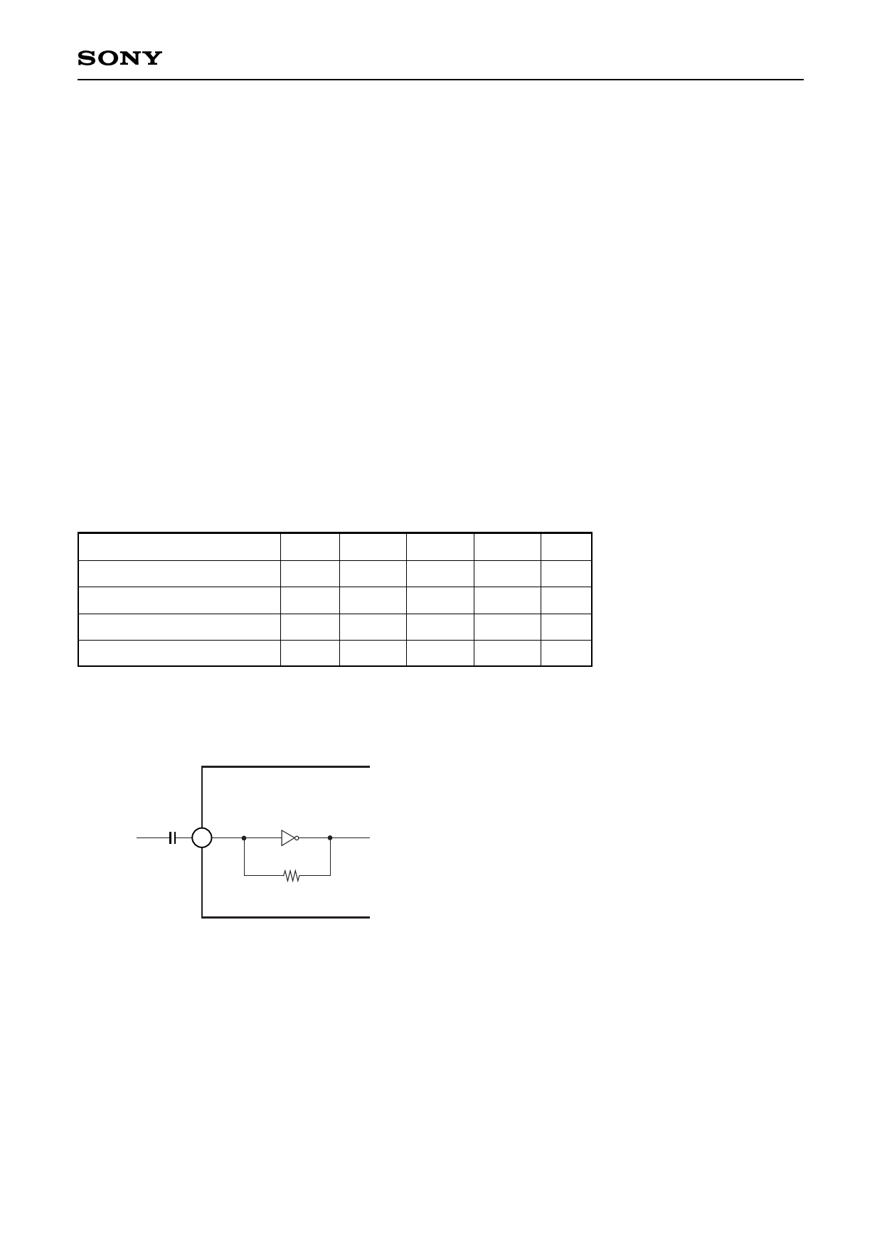
Applicable pins: PECLCK (Pin 2)
∗1 Input the signal through a capacitor. Also, this amplitude is the value between the through capacitor and the
input pin.
PECLCK
2
– 10 –
Share Link: 