UPD488448FF-C80-45-DQ2 データシートの表示(PDF) - NEC => Renesas Technology
部品番号
コンポーネント説明
メーカー
UPD488448FF-C80-45-DQ2 Datasheet PDF : 80 Pages
| |||
µPD488448 for Rev. P
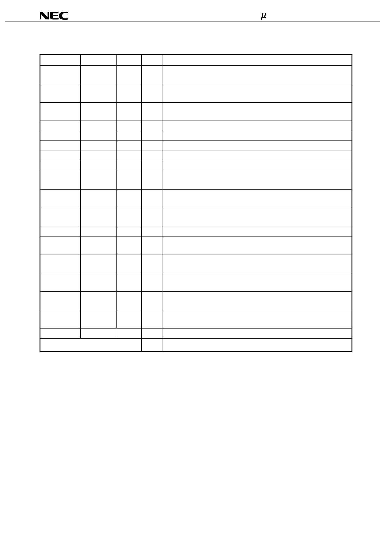
Pin Description
Signal
Input / Output Type #pins
Description
SIO0, SIO1
CMD
SCK
Input / Output CMOS Note1 2
Input
CMOS Note1
1
Input
CMOS Note1
1
Serial input/output. Pins for reading from and writing to the control registers using
a serial access protocol. Also used for power management.
Command input. Pins used in conjunction with SIO0 and SIO1 for reading from
and writing to the control registers. Also used for power management.
Serial clock input. Clock source used for reading from and writing to the control
registers.
VDD
10 Supply voltage for the RDRAM core and interface logic.
VDDa
1 Supply voltage for the RDRAM analog circuitry.
VCMOS
2 Supply voltage for CMOS input/output pins.
GND
13 Ground reference for RDRAM core and interface.
GNDa
1 Ground reference for RDRAM analog circuitry.
DQA7..DQA0 Input / Output RSL Note2
CFM
Input
RSL Note2
CFMN
Input
RSL Note2
8 Data byte A. Eight pins which carry a byte of read or write data between the
Channel and the RDRAM.
1 Clock from master. Interface clock used for receiving RSL signals from the
Channel. Positive polarity.
1 Clock from master. Interface clock used for receiving RSL signals from the
Channel. Negative polarity.
VREF
1 Logic threshold reference voltage for RSL signals.
CTMN
Input
RSL Note2
CTM
Input
RSL Note2
RQ7..RQ5 or
ROW2..ROW0
RQ4..RQ0 or
COL4..COL0
DQB7..DQB0
Input
RSL Note2
Input
RSL Note2
Input / Output RSL Note2
1 Clock to master. Interface clock used for transmitting RSL signals to the Channel.
Negative polarity.
1 Clock to master. Interface clock used for transmitting RSL signals to the Channel.
Positive polarity.
3 Row access control. Three pins containing control and address information for
row accesses.
5 Column access control. Five pins containing control and address information for
column accesses.
8 Data byte B. Eight pins which carry a byte of read or write data between the
Channel and the RDRAM.
NC
2 These pins aren’t connected to inside of the chip.
Total pin count per package
62
Notes 1.All CMOS signals are high-true ; a high voltage is a logic one and a low voltage is logic zero.
2.All RSL signals are low-true ; a low voltage is a logic one and a high voltage is logic zero.
Data Sheet M14837EJ3V0DS00
5
Share Link: 