ST95P04 データシートの表示(PDF) - STMicroelectronics
部品番号
コンポーネント説明
メーカー
ST95P04 Datasheet PDF : 16 Pages
| |||
ST95P04
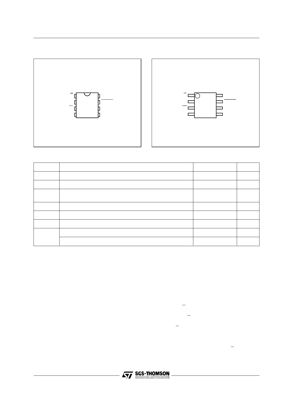
Figure 2A. DIP Pin Connections
ST95P04
S1
Q2
8 VCC
7 HOLD
W3
6C
VSS 4
5D
AI01064B
Figure 2B. SO Pin Connections
S
Q
W
VSS
ST95P04
1
8
2
7
3
6
4
5
AI01065C
VCC
HOLD
C
D
Table 2. Absolute Maximum Ratings (1)
Symbol
Parameter
Value
Unit
TA
Ambient Operating Temperature
–40 to 85
°C
TSTG
Storage Temperature
–65 to 150
°C
TLEAD Lead Temperature, Soldering
(SO8 package)
40 sec
215
(PSDIP8 package) 10 sec
260
°C
VO
Output Voltage
–0.3 to VCC +0.6
V
VI
Input Voltage
–0.3 to 6.5
V
VCC
VESD
Supply Voltage
Electrostatic Discharge Voltage (Human Body model) (2)
Electrostatic Discharge Voltage (Machine model) (3)
–0.3 to 6.5
V
4000
V
500
V
Notes: 1. Except for the rating "Operating Temperature Range", stresses above those listed in the Table "Absolute Maximum Ratings"
may cause permanent damage to the device. These are stress ratings only and operation of the device at these or any other
conditions above those indicated in the Operating sections of this specification is not implied. Exposure to Absolute Maximum
Rating conditions for extended periods may affect device reliability. Refer also to the SGS-THOMSON SURE Program and
other relevant quality documents.
2. MIL-STD-883C, 3015.7 (100pF, 1500Ω)
3. EIAJ IC-121 (Condition C) (200pF, 0Ω)
SIGNALS DESCRIPTION
Serial Output (Q). The output pin is used to trans-
fer data serially out of the ST95P04. Data is shifted
out on the falling edge of the serial clock.
Serial Input (D). The input pin is used to transfer
data serially into the device. It receives instructions,
addresses, and data to be written. Input is latched
on the rising edge of the serial clock.
Serial Clock (C). The serial clock provides the
timing of the serial interface. Instructions, ad-
dresses, or data present at the input pin are latched
on the rising edge of the clock input, while data on
the Q pin changes after the falling edge of the clock
input.
Chip Select (S). This input is used to select the
ST95P04. The chip is selected by a high to low
transition on the S pin when C is at ’0’ state. At any
time, the chip is deselected by a low to high transi-
tion on the S pin when C is at ’0’ state. As soon as
the chip is deselected, the Q pin is at high imped-
ance state. This pin allows multiple ST95P04 to
share the same SPI bus. After power up, the chip
is at the deselect state. Transitions of S are ignored
when C is at ’1’ state.
2/16
Share Link: 