ST95P04 データシートの表示(PDF) - STMicroelectronics
部品番号
コンポーネント説明
メーカー
ST95P04 Datasheet PDF : 16 Pages
| |||
ST95P04
Read Status Register (RDSR)
The RDSR instruction provides access to the status
register. The status register may be read at any
time, even during a non-volatile write. As soon as
the 8th bit of the status register is read out, the
ST95P04 enters a wait mode (data on D are not
decoded, Q is in Hi-Z) until it is deselected.
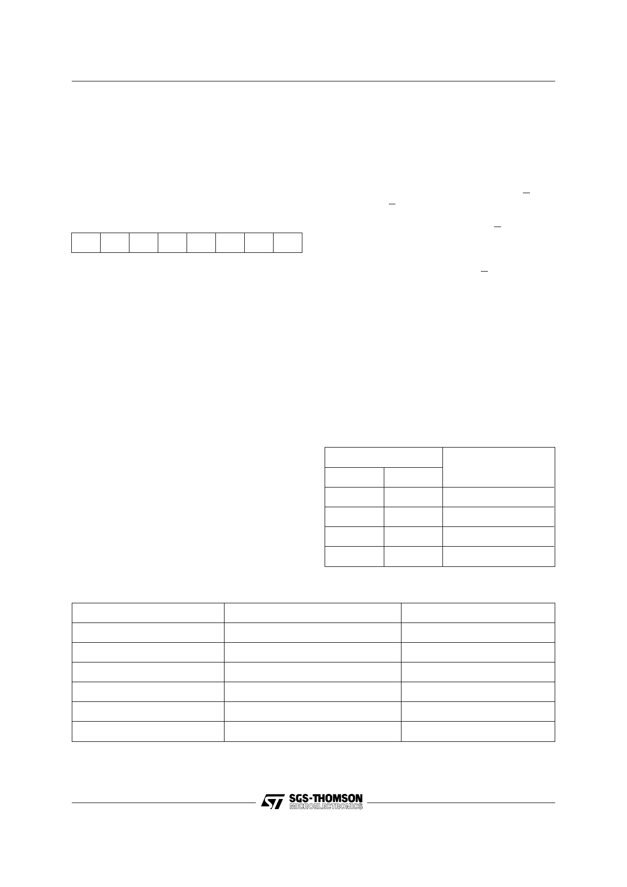
The status register format is as follows:
b7
b0
1
1
1
1 BP1 BP0 WEL WIP
BP1, BP0: Read and Write bits
WEL, WIP: Read only bits.
During a non-volatile write to the memory array, all
bits BP1, BP0, WEL, WIP are valid and can be read.
During a non volatile write to the status register, the
only bits WEL and WIP are valid and can be read.
The values of BP1 and BP0 read at that time
correspond to the previous contents of the status
register.
The Write-In-Process (WIP) read only bit indicates
whether the ST95P04 is busy with a write opera-
tion. When set to a ’1’ a write is in progress, when
set to a ’0’ no write is in progress.
The Write Enable Latch (WEL) read only bit indi-
cates the status of the write enable latch. When set
to a ’1’ the latch is set, when set to a ’0’ the latch is
reset.
The Block Protect (BP0 and BP1) bits indicate the
extent of the protection employed. These bits are
set by the user issuing the WRSR instruction.
These bits are non-volatile.
Write Status Register (WRSR)
The WRSR instruction allows the user to select the
size of protected memory. The ST95P04 is divided
into four 1024 bit blocks. The user may read the
blocks but will be unable to write within the selected
blocks.
The blocks and respective WRSR control bits are
shown in Table 6.
When the WRSR instruction and the 8 bits of the
Status Register are latched-in, the internal write
cycle is then triggered by the rising edge of S. This
rising edge of S must appear after the 8th bit of the
Status Register content (it must not appear a 17th
clock pulse before the rising edge of S), otherwise
the internal write sequence is not performed.
Read Operation
The chip is first selected by putting S low. The serial
one byte read instruction is followed by a one byte
address (A7-A0), each bit being latched-in during
the rising edge of the clock (C). Bit 3 of the read
instruction contains address A8 (most significant
address bit). This bit is used to select the first or
second page of the device. Then, the data stored
in the memory at the selected address is shifted out
on the Q output pin; each bit being shifted out
during the falling edge of the clock (C). The data
stored in the memory at the next address can be
read in sequence by continuing to provide clock
Table 6. Array Addresses Protect
Status Register Bits
BP1
BP0
Array Addresses
Protected
0
0
0
1
1
0
none
180h - 1FFh
100h - 1FFh
1
1
000h - 1FFh
Table 7. Instruction Set
Instruction
WREN
WRDI
RDSR
WRSR
READ
WRITE
Notes: A = 1, Upper page selected
A = 0, Lower page selected
X = Don’t care
8/16
Description
Set Write Enable Latch
Reset Write Enable Latch
Read Status Register
Write Status Register
Read Data from Memory Array
Write Data to Memory Array
Instruction Format
0000 X110
0000 X100
0000 X101
0000 X001
0000 A011
0000 A010
Share Link: 