VES1820X データシートの表示(PDF) - Philips Electronics
部品番号
コンポーネント説明
メーカー
VES1820X Datasheet PDF : 40 Pages
| |||
Philips Semiconductors
Single chip DVB-C channel receiver
Product specification
VES1820X
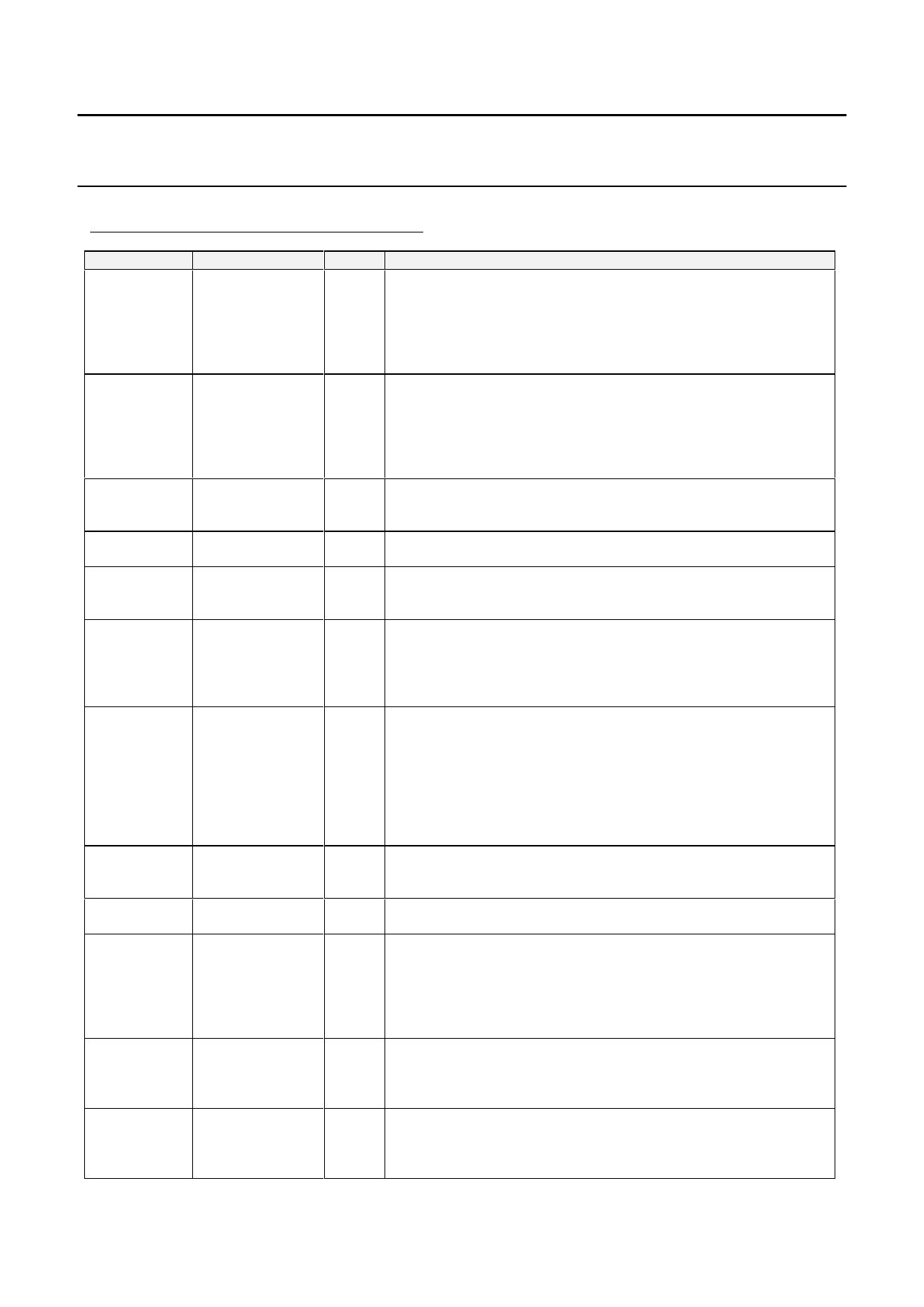
INPUT - OUTPUT SIGNAL DESCRIPTION
SYMBOL
CLR#
XIN
XOUT
SACLK
FI[8:0]
VAGC
DO[7:0]
OCLK
DEN
UNCOR
PSYNC
TESTO[16:0]
PIN NUMBER
27
2
3
18
5,6,7,8,12,
13,14,15,16
20
46,49,50,51
52,53,54,55
44
45
42
43
78,77,76,75,74
71,70,69,68,67
64,63,62,61,60
57,56
TYPE
I
I
O
O
(5V)
I
O
(5V)
O
(3.3V)
O
(3.3V)
O
(3.3V)
O
(3.3V)
O
(3.3V)
O
(3.3V)
DESCRIPTION
The CLR# input is asynchronous and active low, and clears the
VES1820X. When CLR# goes low, the circuit immediately enters its
RESET mode and normal operation will resume 4 XIN falling edges
later after CLR# returned high. The I2C register contents are all
initialized to their default values. The minimum width of CLR# at low
level is 4 XIN clock periods.
XTAL oscillator input pin. Typically a fundamental XTAL oscillator is
connected between the XIN and XOUT pins (see typical application
on FIGURE 10 page 15). The XTAL frequency MUST be chosen so
that the system frequency SYSCLK (= XIN * multiplying factor of the
PLL) equals to 1.6 times the tuner output Intermediate Frequency :
SYSCLK = 1.6 x IF.
XTAL oscillator output pin. Typically a fundamental XTAL oscillator is
connected between the XIN and XOUT pins (see typical application
FIGURE 10 page 15).
Sampling CLocK. This output clock can be fed to an external 9-bit
ADC as the sampling clock.SACLK = SYSCLK/2.
FI [8:0] is the 9-bit input of the IF signal. FI[8:0] is the output of an
external A/D converter. FI[8] is the MSB. When not used, must be
tied to ground.
PWM encoded output signal for AGC. This signal is typically fed to
the AGC amplifier through a single RC network (see typical
application FIGURE 11 page 16). The maximum signal frequency on
VAGC output is XIN/16. AGC information is refreshed every 1024
symbols.
Data Output bus . These 8-bit parallel data are the outputs of the
VES1820X after demodulation, de-interleaving, RS decoding and de-
scrambling.
When one of the two possible parallel interfaces is selected
(Parameter SERINT=0, index 2016) then DO[7:0] is the transport
stream output.
When the serial interface is selected (Parameter SERINT=1, index
2016) then the serial output is on pin DO[0] (pin 55).
Output CLock. OCLK is the output clock for the parallel DO[7:0]
outputs. OCLK is internally generated depending on which interface
is selected.
Data ENable : this output signal is high when there is a valid data on
output bus DO[7 :0].
UNCORrectable packet. This output signal is high when the provided
packet is uncorrectable (during the 188 bytes of the packet). The
uncorrectable packet is not affected by the Reed Solomon decoder,
but the MSB of the byte following the sync. byte is forced « 1 » for
the MPEG2 process : Error Flag Indicator (if RSI and IEI are set low
in the I2C table).
Pulse SYNChro. This output signal goes high when the sync byte
(4716) is provided, then it goes low until the next sync byte. If the
serial interface is selected, then PSYNC is high only during the first
bit of the sync byte (4716). See FIGURE 8 page 14.
TESTO [16:0] is 17-bit Test output bus.
1999 March 01
7
Share Link: 