BA17806T データシートの表示(PDF) - ROHM Semiconductor
部品番号
コンポーネント説明
メーカー
BA17806T Datasheet PDF : 11 Pages
| |||
Regulator ICs
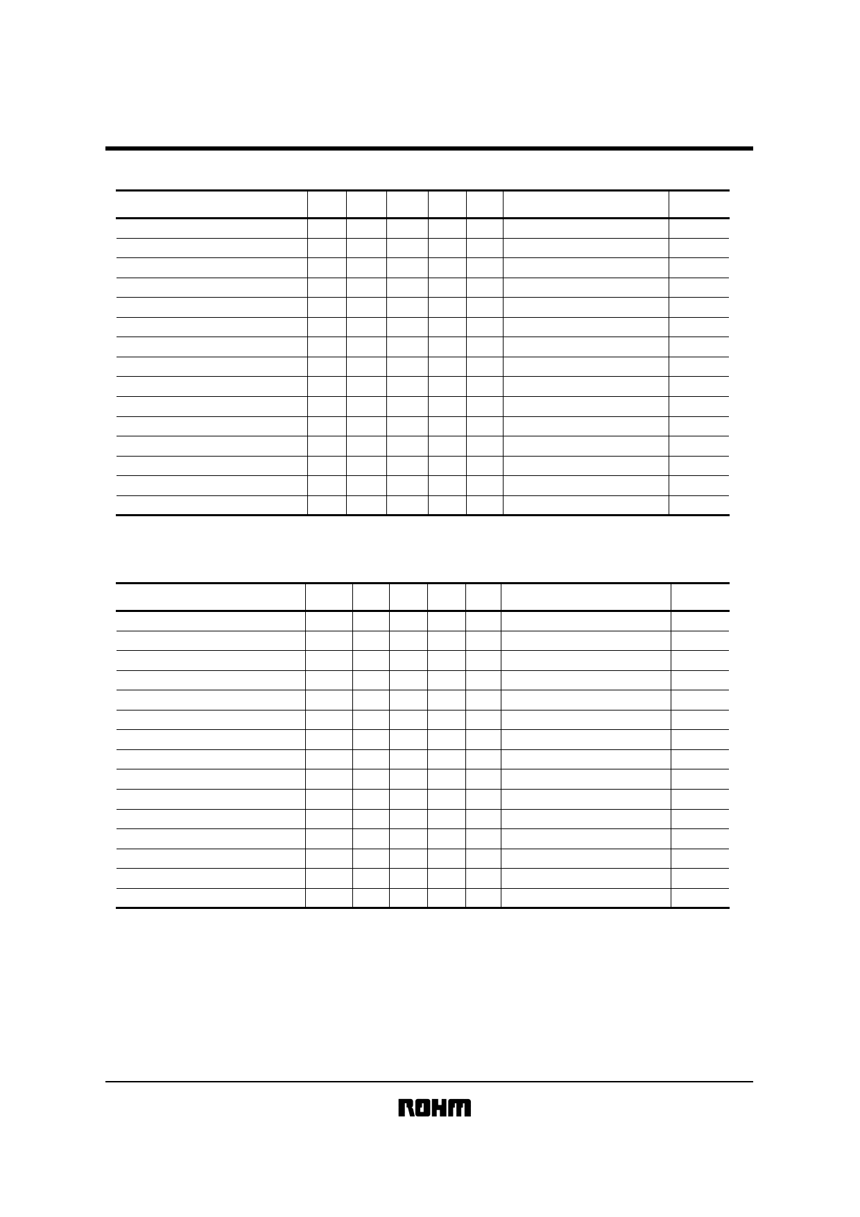
BA178!!T / FP series
<BA17808T / FP individual specifications> (unless otherwise noted, Ta=25°C, VIN=14V, IO=500mA)
Parameter
Symbol Min.
Output voltage 1
VO1 7.7
Output voltage 2
VO2 7.6
Input stability 1
Reg.I1 −
Input stability 2
Reg.I2 −
Ripple rejection ratio
R.R. 56
Load regulation 1
Reg.L1 −
Load regulation 2
Reg.L2 −
Temperature coefficient of output voltage TCVO −
Output noise voltage
Vn
−
Minimum I/O voltage differential
Vd
−
Bias current
Ib
−
Bias current change 1
Ib1
−
Bias current change 2
Ib2
−
Peak output current
IO-P
−
Output short-circuit current
IOS
−
Typ.
8.0
−
5
3
65
19
7
−0.5
80
2.0
4.5
−
−
1.7
0.6
Max. Unit
Conditions
8.3 V IO=500mA
8.4 V VIN=10.5∼23V, IO=5mA∼1A
160 mV VIN=10.5∼25V, IO=500mA
80 mV VIN=11∼17V, IO=500mA
−
dB eIN=1Vrms, f=120Hz, IO=100mA
160 mV IO=5mA∼1A
80 mV IO=250∼750mA
− mV/˚C IO=5mA, Tj=0∼125˚C
− µV f=10Hz∼100kHz
−
V IO=1A
8.0 mA IO=0mA
0.5 mA IO=5mA∼1A
0.8 mA VIN=10.5∼25V
−
A Tj=25˚C
−
A VIN=25V
Measurement
circuit
Fig.1
Fig.1
Fig.1
Fig.1
Fig.2
Fig.1
Fig.1
Fig.1
Fig.3
Fig.4
Fig.5
Fig.5
Fig.5
Fig.1
Fig.6
<BA17809T / FP individual specifications> (unless otherwise noted, Ta=25°C, VIN=15V, IO=500mA)
Parameter
Symbol Min.
Output voltage 1
VO1
Output voltage 2
VO2
Input stability 1
Reg.I1
Input stability 2
Reg.I2
Ripple rejection ratio
R.R.
Load regulation 1
Reg.L1
Load regulation 2
Reg.L2
Temperature coefficient of output voltage TCVO
Output noise voltage
Vn
Minimum I/O voltage diffrential
Vd
Bias current
Ib
Bias current change 1
Ib1
Bias current change 2
Ib2
Peak output current
IO-P
Output short-circuit current
IOS
8.6
8.55
−
−
56
−
−
−
−
−
−
−
−
−
−
Typ.
9.0
−
6
4
64
20
8
−0.5
90
2.0
4.5
−
−
1.7
0.3
Max. Unit
Conditions
Measurement
circuit
9.4 V IO=500mA
Fig.1
9.45 V VIN=11.5∼26V, IO=5mA∼1A
Fig.1
180 mV VIN=11.5∼26V, IO=500mA
Fig.1
90 mV VIN=13∼19V, IO=500mA
Fig.1
−
dB eIN=1Vrms, f=120Hz, IO =100mA
Fig.2
180 mV IO=5mA∼1A
Fig.1
90 mV IO=250∼750mA
Fig.1
− mV/˚C IO=5mA, T j =0∼125˚C
Fig.1
− µV f=10Hz∼100kHz
Fig.3
−
V IO=1A
Fig.4
8.0 mA IO=0mA
Fig.5
0.5 mA IO=5mA∼1A
Fig.5
0.8 mA VIN=11.5∼26V
Fig.5
−
A Tj=25˚C
Fig.1
−
A VIN=30V
Fig.6
Share Link: 