LTC1623 データシートの表示(PDF) - Linear Technology
部品番号
コンポーネント説明
メーカー
LTC1623 Datasheet PDF : 12 Pages
| |||
LTC1623
APPLICATIONS INFORMATION
To avoid turning on the external power MOSFETs too
quickly, an internal 10k resistor has been placed in series
with each of the output gate drive pins (see Functional
Block Diagram). Therefore, it only needs an external 0.1µF
capacitor to create enough RC delay (10k • 0.1µF = 1ms)
to slow down the ramp rate of the output gate drive. In
other words, it will take a minimum of 1ms to charge up
the external MOSFET. An additional external 1k resistor
between the 0.1µF capacitor and the gate of the MOSFET
(Figure 3) is required to eliminate possible MOSFET self
oscillations.
For active-low applications in which the load needs to be
on upon power-up, an external P-channel switch can be
used (Figure 3). This load can be switched off later after the
proper protocol has been sent.
Used with the LT®1431, the LTC1623 makes a 3.3V/3A
extremely low voltage drop regulator (Figures 4 and 5). In
this application, the other output channel can be used to
drive a separate load, or it can also be used to control the
output of the LDO so that the user has total control over the
switching in and switching out of the LDO (Figure 5). Also,
with the help of the LT1304-5, the LTC1623 can be used
to make a boost switching regulator with a low standby
current of 22µA (Figure 6).
VCC
2.7V TO 5.5V
(FROM
SMBus)
10µF
(PROGRAMMABLE)
VCC
CLK
GA
DATA
LTC1623 GB
AD0
AD1
GND
1k
0.1µF
Q1
Si3442DV
1k
0.1µF
Q2
Si6433DQ
DISPLAY
FAN
1623 F03
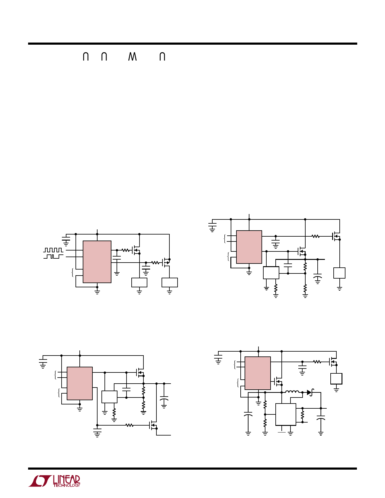
Figure 3. Dual Load Switch with Q2 On upon Power-Up
VCC
3.5V TO 5.5V
10µF
(FROM SMBus)
(PROGRAMMABLE)
CLK VCC GA
DATA
LTC1623
AD0
GB
AD1
GND
0.1µF
13
LT1431 8
510pF
56
680Ω
1k
Si3442DV
Si3442DV
3.3k
+
VOUT
3.3V
470µF LOAD
6V
10k
1623 F04
Figure 4. 3.3V/3A Extremely Low Voltage Drop
Regulator and Load Switch
VCC
3.5V TO 5.5V
10µF
(FROM SMBus)
(PROGRAMMABLE)
CLK VCC GA
DATA
LTC1623
AD0
GB
AD1
GND
Si3442DV
13
LT1431 8
510pF 3.3k
56
10k
680Ω
VOUT
3.3V
+ 470µF
6V
1k
0.1µF
Si3442DV
1623 TA03
SWITCHED
VOUT
3.3V
Figure 5. SMBus Controlled Low Dropout Regulator
VCC
2.7V TO 4.5V
10µF
(FROM
SMBus)
(PROGRAMMABLE)
CLK VCC GA
DATA
LTC1623
AD0
GB
AD1 GND
1k
0.1µF
Si3442DV
22µH*
1N5817
Si3442DV
LOAD
*SUMIDA CD54-220
34
+
499k
8
100µF
LT1304-5
2
604k
100k +
LBO
5V
200mA
2200µF
75
SHDN
1623 F05
Figure 6. Switching Regulator with Low-Battery
Detect Using 22µA Standby Current
9
Share Link: 