NJG1312PC1-C7 データシートの表示(PDF) - Japan Radio Corporation
部品番号
コンポーネント説明
メーカー
NJG1312PC1-C7 Datasheet PDF : 7 Pages
| |||
NJG1312PC1
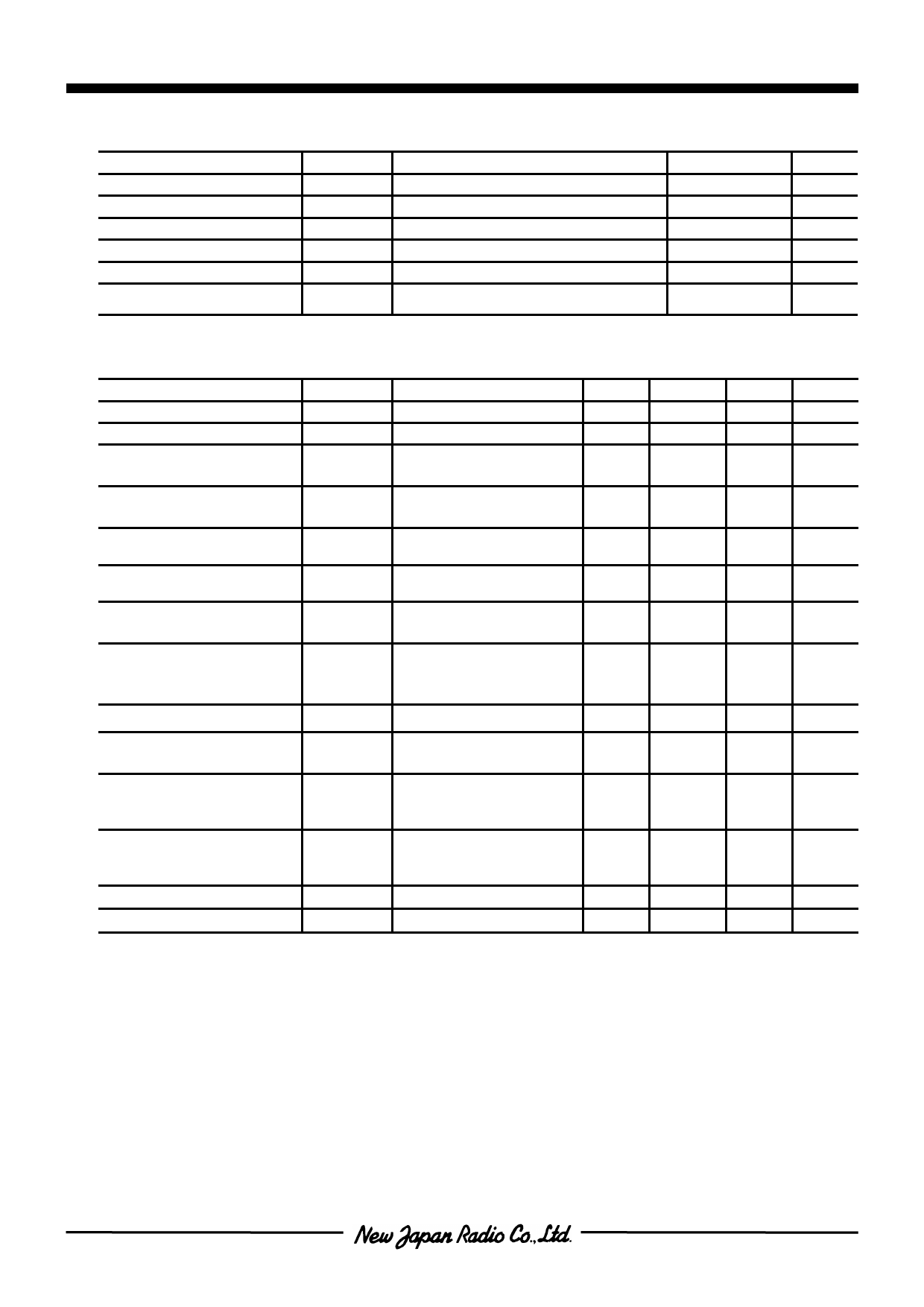
nABSOLUTE MAXIMUM RATINGS
PARAMETER
Drain Voltage
Control Voltage
Input Power
Power Dissipation
Operating Temperature
Storage Temperature
SYMBOL
VDD
VCTL
Pin
PD
Topr
Tstg
CONDITIONS
VDD=2.9V
(Ta=+25°C, Zs=Zl=50Ω)
RATINGS UNITS
6
V
6
V
15
dBm
400
mW
-40~+85
°C
-55~+125
°C
nELECTRICAL CHARACTERISTICS
(VDD=2.9V, VCTR=2.7V, f=900MHz, Ta=-20~+80°C, Zs=Zl=50Ω, Rs (External)=180Ω)
PARAMETER
SYMBOL
CONDITIONS
MIN TYP MAX UNITS
Operating Frequency
Freq
887 900 925 MHz
Drain Voltage
Operating Current
VDD
IDD
RF SW ON
Pout=+5.6dBm
2.7
2.9
5.0
V
−
17
22 mA
Control Current
ICTL
−
1.0
2.0
uA
Control Voltage(LOW)
VCTL(L)
-0.2
0
0.2
V
Control Voltage(HIGH)
Small Signal Gain
Gain Flatness
VCTL(H)
Gain
Gflat
RF SW ON
Pin=-15dBm
RF SW ON
Pin=-15dBm
f=887~925MHz
2.5
2.7
5.5
V
17
19
22
dB
−
0.5
−
dB
Gain Control Range
Pout at 1dB Gain
Compression point
IN-Band Spurious1
IN-Band Spurious2
Input VSWR
Output VSWR
Gcont
P-1dB
IBS1
IBS2
VSWRi
VSWRo
Pin=-15dBm
RF SW ON
RF SW ON,
Pout=+5.6dBm
OFFSET 900kHz
RF SW ON,
Pout=+5.6dBm
OFFSET 1.98MHz
RF SW ON
RF SW ON
-28.5 -27 -25.5 dB
−
+10
−
dBm
−
-55
-51 dBc
−
-73
-68 dBc
−
2.4
3.0
−
1.4
2.0
Note) RF SW ON/OFF in the table above: Control voltages (V CTL1, V CTL2) are as follows
RF SW ON
RF SW OFF
P1: V CTL1=0V, V CTL2=2.7V
P2: V CTL1=2.7V, V CTL2=0V
P1: V CTL1=2.7V, V CTL2=0V
P2: VCTL1=0V, VCTL2=2.7V
-2-
Share Link: 