PBD3517-1 データシートの表示(PDF) - Ericsson
部品番号
コンポーネント説明
メーカー
PBD3517-1 Datasheet PDF : 10 Pages
| |||
PBD 3517/1
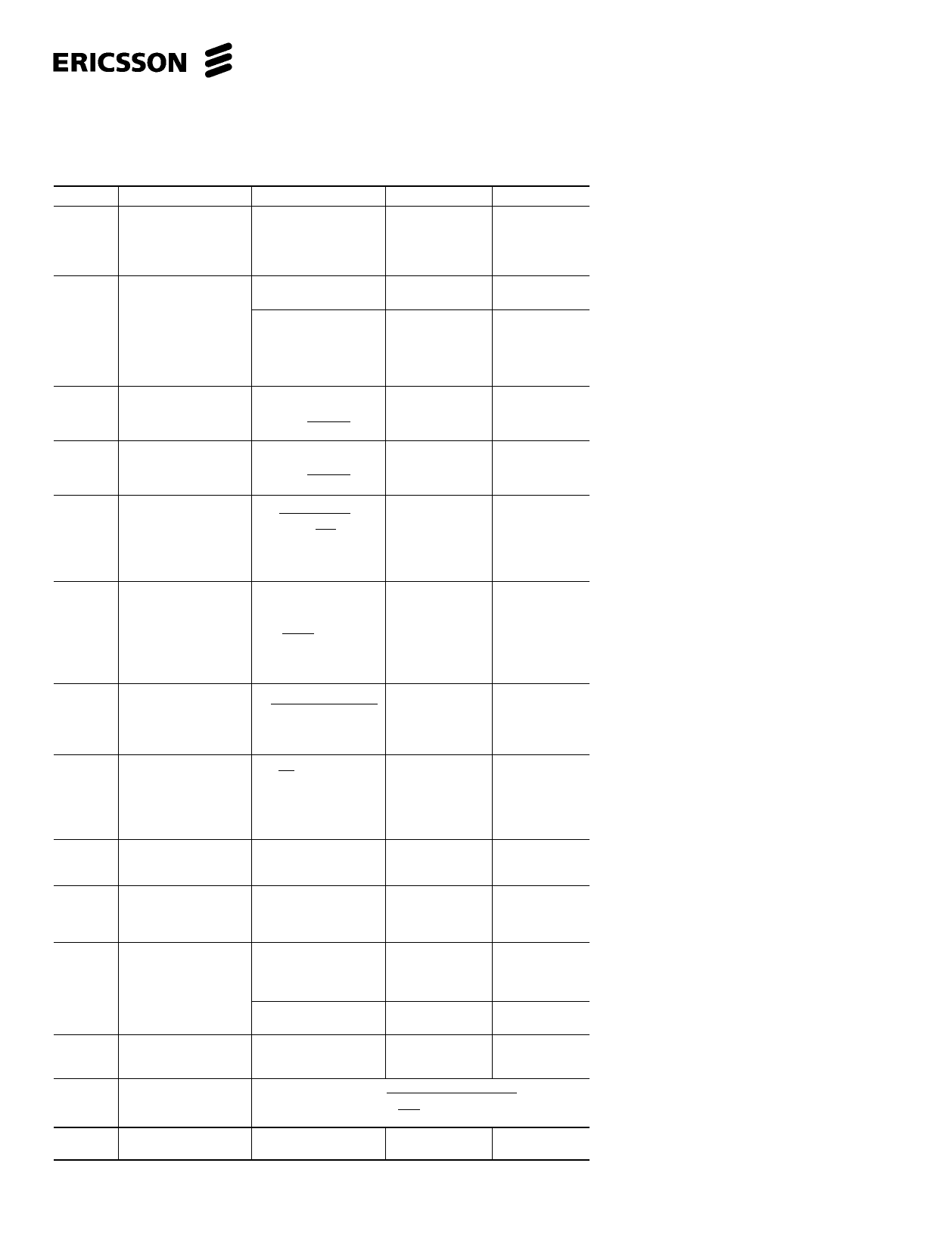
Purpose of external components
For figures 14 and 15. Note that “Larger than …” is normally the vice versa of “Smaller
than … .”
Component Purpose
Value
Larger than value Smaller than value
D1, D2
Passes low power to
motor and prevents
high power from
shorting through low
power supply
If = 1A
1N4001, UF4001
Increases price
Decreases max
current capability
D3 … D6
Inductive current
supressor
If = 1A
Increases price
Decreases current
turn-off capability
trr = 100nS
e.g.
BYV27
UF4001
RGPP10G
RGPP30D
Slows down turn-
off time. Voltage
at anode might
exceed voltage
breakdown
Speeds up turn-
off time.
R1
R2, R3
R4 … R7
Base drive current
limitter
R = 20ohm
( ) P = R1
Vmm 2
R1 + R2
Base discharge resistor R = 240ohm
( ) P = R1
Vmm 2
R1 + R2
( ) External transistor base
driver
R
=
Vmm-
Vbe- Vce
Vbe
I4 - R12
P > (I4)2• R4
Check hfe.
Slows down Q1’s Speeds up Q1’s
turn-on and Q4’s turn-on and Q4’s
turn-off time.
turn-off time.
Slows down Q1’s Speeds up Q1’s
turn-off and Q4’s turn-off and Q4’s
turn-on time.
turn-on time.
Decreases ext. Increases ext.
transistor IC max. transistor IC max.
Lowers 3517
Increases 3517
power dissipation. power dissipation.
R8, R9
ØA, ØB pull-up
resistors
R = 5ohm @ pull-up
voltage = 5V.
(VCC)2
P=
R
Increases noise
sensitivity, worse
logic-level
definition
Increases noise
immunity, better
logic-level
definition.
Less stress on ØA, Stress on ØA, ØB
ØB output
output
transistors
transistors.
R10, R11
Limit max. motor
Vmm-VMotor -VCESat
current. Resistors may R =
be omitted. (Check
IMotor max
motor specifications
first.)
Decreases motor
current.
Increases motor
current.
R12 … R15 External transistor base
Vbe
R= ª
discharge.
I12
15W
P > Vbe• I12
Slows down
Speeds up
external transistor external transistor
turn-off time.
turn-off time.
Lowers 3517
Increases 3517
power dissipation power dissipation
RT, CT
C1, C2
C3 … C5
Q1, Q2
Q3, Q4
Q5 … Q8
Sets LA and LB on time R = 47kohm, C = 10nf
when triggered by
STEP.
P < 250mW
Increases on time. Decreases on time.
Stores the doubling
voltage.
C = 100µ F
VC ≥ 45V
Increases effective
on-time during
voltage doubling
Decreases
effective on-time
during voltage
doubling.
Filtering of supply-
C ≥ 10 µF
voltage ripple and take-
up of energy feedback
from D3 … D6
Increases price,
better filtering,
decreases risk of
IC breakdown
Decreases price,
more compact
solution.
VRated>Vmm ,Vss or Vcc Increases price
Risk for capacitor
breakdown.
Activation transistor of IC as motor requires.
voltage doubling.
Increases price.
Decreases max Im
during voltage
doubling.
Charging of voltage
doubling capacitor
( ) IC=
(Vmm- Vf -VCE ) • C1
1
-
fStep
0.55
•
RT •
CT
Motor current drive
transistor.
IC as motor requires.
PNP power trans.
Increases max
Decreases max
current capability. current capability.
INH — Inhibit
A HIGH level on the INH input,turns off all
phase outputs to reduce current
consumption.
Reset
An internal Power-On Reset circuit
connected to Vcc resets the phase logic
and inhibits the outputs during power up,
to prevent false stepping.
Output Stages
The output stage consists of four open-
collector transistors. The second high-
voltage supply contains Darlington
transistors.
Phase Outputs
The phase outputs are connected directly
to the motor as shown in figure 14.
Bilevel Technique
The bilevel pulse generator consists of
two monostables with a common RC
network.
The internal phase logic generates a
trigger pulse every time the phase
changes state. The pulse triggers its own
monostable which turns on the output
transistors for a precise period of time:
tOn = 0.55 • CT • RT.
See pulse diagrams, figures 16 through
20.
Bipolar Phase Logic Output
The ØA and ØB outputs are generated
from the phase logic and inform an
external device if the A phase or the B
phase current is internally inhibited.
These outputs are intended to support if it
is legal to correctly go from a half-step
mode to a full-step mode without loosing
positional information.
The PBD 3517/1 can act as a controller
IC for 2 driver ICs, the PBL 3770A. Use
PA1 and PB1 for phase control, and ØA and
ØB for I0 and I1 control of current turn-off.
Applications Information
Logic inputs
If any of the logic inputs are left open, the
circuit will treat it as a high-level input.
Unused inputs should be connected to
proper voltage levels in order to get the
highest noise immunity.
Phase outputs
7
Share Link: 